
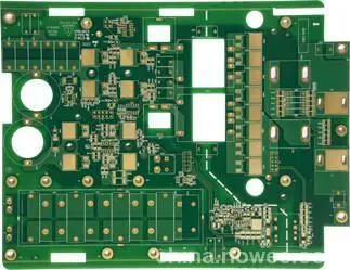
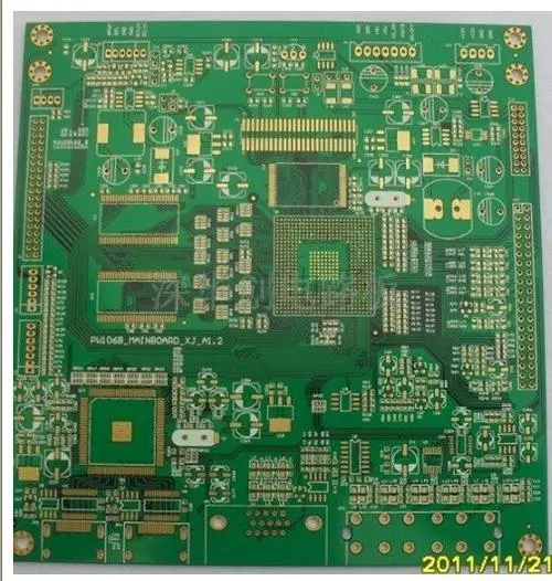
Professional PCB manufacturing and assembly
Building 6, Zone 3, Yuekang Road,Bao'an District, Shenzhen, China
+86-13410863085Mon.-Sat.08:00-20:00

There are three reasons for the welding defects of circuit boards:
1. Solderability of PCB holesaffects welding quality
Poor solderability of circuit board holes will lead to faulty soldering defects, which will affect the parameters of components in the circuit, lead to unstable conduction of components and inner wires of multilayer board, and cause the functional failure of the whole circuit. Solderability is the property that the metal surface is wetted by molten solder, that is, a relatively uniform, continuous and smooth adhesive film is formed on the metal surface where the solder is located.
The factors that affect the solderability of PCB mainly include: (1) the composition of solder and the properties of solder. Solder is an important part of welding chemical treatment process. It is composed of chemical materials containing flux. The commonly used low melting point eutectic metal is Sn Pb or Sn Pb Ag The impurity content shall be controlled in proportion to prevent the oxide produced by impurities from being dissolved by the flux. The function of the flux is to help the solder to wet the circuit surface of the soldered board by transferring heat and removing rust. White rosin and isopropanol solvent are generally used.
(2) The weldability is also affected by the welding temperature and the cleanliness of the metal plate surface. If the temperature is too high, the solder diffusion speed will be accelerated. At this time, the solder has high activity, which will cause rapid oxidation of the circuit board and solder melting surface, resulting in welding defects. If the circuit board surface is polluted, the solderability will also be affected, resulting in defects. These defects include solder beads, solder balls, open circuit, poor gloss, etc.
2. PCB welding defects caused by warping
The circuit board and components are warped during welding, and defects such as false soldering and short circuit are caused due to stress deformation. Warpage is often caused by the temperature imbalance between the upper and lower parts of the circuit board. For large PCBs, warping will also occur due to the weight of the board itself. Ordinary PBGA devices are about 0.5mm away from the printed circuit board. If the components on the circuit board are large, the solder joints will be under stress for a long time as the circuit board returns to its normal shape after cooling down. If the components are raised by 0.1mm, it will be enough to cause open circuit due to faulty soldering.
3. PCB design affects welding quality
In PCB layout, when the size of the circuit board is too large, although the welding is easier to control, the printing line is long, the impedance increases, the noise resistance decreases, and the cost increases; If it is too small, the heat dissipation will drop, the welding is not easy to control, and the adjacent lines will easily interfere with each other, such as the electromagnetic interference of the circuit board. Therefore, PCB design must be optimized:
(1) Shorten the connection between high-frequency components and reduce EMI interference.
(2) Components with large weight (such as more than 20g) shall be fixed with supports and then welded
(3) Heat dissipation shall be considered for heating elements to prevent large Δ In case of defects and rework, the thermal sensor shall be far away from the heat source.
(4) The arrangement of elements shall be as parallel as possible, which is not only beautiful but also easy to weld, and it is suitable for mass production. The PCB designed as a 4 ∶ 3 rectangle. The wire width shall not change suddenly to avoid the discontinuity of PCB wiring. When the circuit board is heated for a long time, the copper foil is easy to expand and fall off. Therefore, large area copper foil should be avoided.


Just upload Gerber files, BOM files and design files, and the KINGFORD team will provide a complete quotation within 24h.