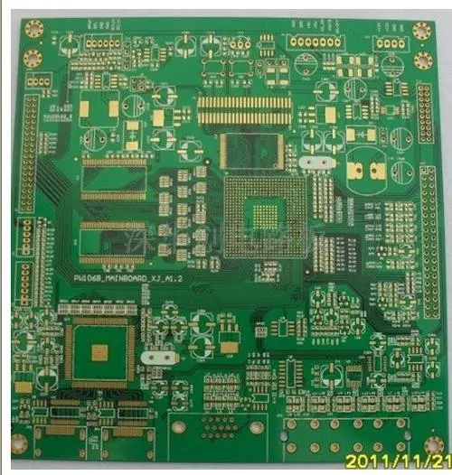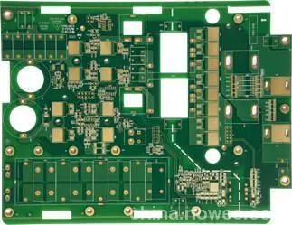
In the automatic surface mounting line, if the circuit board is not flat, it will lead to inaccurate positioning, and the components cannot be inserted or mounted to the holes and surface mounting pads of the board, or even damage the automatic mounting machine.
After the circuit board is connected with the components, it will bend, and the component pins are not easy to be cut flat. The board cannot be put into the chassis or socket, so the assembly plant is also very worried about the board warping.
The current surface mount technology is developing in the direction of high precision, high speed and intelligence, which requires PCB board to have higher flatness and can be used as the main component of various components.

In particular, IPC standards specify that the allowable deformation of PCB boards with surface mount devices is 0.75%, while the allowable deformation of PCB boards without surface mount devices is 1.5%.
In practical application, in order to meet the requirements of high-precision and high-speed mounting, some electronic assembly manufacturers have more strict requirements on deformation, such as 0.5% deformation allowance, or even 0.3% for individual requirements.
Printed circuit board is composed of copper foil, resin, glass cloth and other materials. Their physical and chemical properties are different. Pressing together will inevitably produce thermal stress and deformation.
At the same time, during the processing of PCB boards, they will experience various technological processes such as high temperature, mechanical cutting, and wet process, which will also have an important impact on the deformation of the board. The causes of PCB board deformation are complex and changeable. How to reduce or eliminate the deformation caused by different material properties or different processing technologies has become one of the difficulties for PCB manufacturers.
2。
Analysis of the causes of PCB deformation.
The deformation of PCB needs to be studied from several aspects such as material, structure, graphic distribution, PCB processing technology, etc. This paper will analyze and elaborate various causes of possible deformation and improvement methods.
The copper area of the plate is uneven, which makes the plate bending and warping worse.
Usually, a large number of copper foils are designed on the PCB as the grounding, and sometimes a large number of copper foils are designed on the Vcc layer. When these large numbers of copper foils cannot be evenly distributed on the same circuit board, the problem of uneven heat absorption and heat dissipation will occur.
Of course, the circuit board is also heat shrinkable. If the heat shrinkable cannot cause deformation due to different stresses at the same time, then the temperature of the board reaches the upper limit of Tg value, the board will begin to become soft, causing deformation.
The junction point (via) of each layer on the circuit board will limit the lifting of the board.
Most modern circuit boards are multilayer boards. There will be the same junction points as rivets between the boards. The junction points are divided into through holes, blind holes and embedded holes. Where there are junction points, the effect of expansion and contraction of the board will be limited, and the board will be bent and warped indirectly.
Causes of circuit board deformation:
The weight of the circuit board itself will cause the board to sag and deform.
Usually, the reflow furnace adopts a chain structure, which can push the circuit board forward, that is, the whole board should be supported on both sides of the board as a fulcrum.
If there are overweight parts on the plate or the size of the plate is too large, the middle depression will occur due to the number of the plate itself, causing bending.
The depth of V-Cut and the connecting bar will affect the panel deformation.
Fundamentally speaking, V-Cut is the culprit of destroying the plate substructure. Because V-Cut is grooved on the original large plate, it is easy to deform at the V-Cut.
The degree of influence of crimping material, structure and pattern on plate deformation:
The circuit board is formed by pressing core board, prepreg and outer copper foil. The core board and copper foil are subject to thermal deformation during the pressing process, and the deformation amount depends on the thermal expansion coefficient (CTE) of the two materials
The coefficient of thermal expansion (CTE) of copper is about 17X10-6; The coefficient of thermal expansion (CTE) of FR-4 substrate is about (50~70) X10-6; The thermal expansion coefficient (250~350) of common FR-4 base material and X direction CTE are generally similar to copper foil due to the presence of glass cloth
3。
PCB deformation during processing.
The causes of PCB deformation during processing are very complex, which can be divided into thermal stress and mechanical stress.
Among these stresses, thermal stress is generated during pressing, and mechanical stress is generated during stacking, handling and baking of plates. Next, we will have a brief discussion in the order of the process.
1、 Copper clad raw materials:
Copper clad laminate is a double-layer panel with symmetrical structure and no pattern. The CTE of copper foil and glass cloth is far different, so deformation caused by different CTE rarely occurs during pressing.
However, due to the large size of the CCL press and the temperature difference in different areas of the hot plate, there are slight differences in the resin curing speed and degree in different areas during the pressing process. At the same time, there are large differences in dynamic viscosity at different heating rates, which will also produce local stress during the curing process.
Generally, the stress is kept in balance after pressing, but gradually released in the subsequent processing, forming deformation.
2、 Pressing:
The pressing process of printed circuit board is the main process to generate thermal stress. Similar to the pressing process of copper clad plate, it will also generate local stress due to inconsistency during the curing process. Due to the thick thickness of printed circuit board, more patterns, more semi solidified pieces, it is also more difficult to eliminate thermal stress than copper clad plate.
Moreover, the stress on the PCB will be released during the subsequent drilling, forming or baking process, resulting in deformation of the board.
3. Resistance welding, character baking and other processes:
Because PCB solder resist inks cannot overlap each other when curing, the circuit boards are vertically placed on the shelf for drying and curing. The solder resist temperature is about 150 ℃, which just exceeds the Tg point of Tg material. The resin above the Tg point is highly elastic, and the boards are easy to deform under the action of their own weight or strong wind in the oven.
4. Flatness of hot air solder:
Generally, the temperature of the tin furnace of the whole hot air solder machine is 225 ℃~265 ℃, and the time is 3S-6S. The temperature of hot air is 280~300 ℃.
Solder at room temperature shall be sent to the tin furnace from room temperature, and shall be washed with post-treatment water at room temperature within two minutes after being discharged from the furnace. The whole process of hot air solder leveling is a rapid cooling process.
Due to the different materials and uneven structure of PCB, thermal stress will inevitably be generated in the cold and hot process, resulting in micro strain and overall deformation warping area.
5. Storage:
When PCB is stored in the semi-finished product stage, it is usually hard inserted on the shelf. Improper adjustment of shelf tightness or stacking or placing of boards during storage will cause mechanical deformation of the board. Especially, it has a greater impact on the plates below 2.0mm.
In addition to the above factors, there are many other factors that affect the deformation of PCB.
4。
Prevent PCB from warping and deformation.
The warping deformation of PCB has a great impact on the production of PCB, and warping deformation is also an important problem in PCB production. The boards with components will be bent after welding, making the component legs not easy to be neat.
The board cannot be installed on the chassis or socket, so the warping of the circuit board will affect the normal operation of the whole subsequent process.
At present, the printed PCB has entered the stage of surface mounting and chip mounting, and the process requirements are also constantly improving, so the requirements for the warpage of the circuit board are also getting higher and higher. Therefore, we should find out the cause of the half turn.
1、 Engineering design:
Attention shall be paid to the design of printed PCB:
The semi cured sheets between layers shall be arranged symmetrically. For example, the thickness of six layers of plates, 1~2 layers and 5~6 layers of plates shall be consistent with the number of semi cured sheets, otherwise it is easy to delaminate and warp.
Multilayer core boards and semi cured sheets shall be produced by the same supplier.
A. B The linear areas of the two outer planes should be as close as possible. If the A side is large copper and the B side only goes through a few lines, this type of printing plate is easy to warp after etching. If the area difference between two lines is too large, several independent grids can be added on the thin side to achieve balance.


