
Professional PCB manufacturing and assembly
Building 6, Zone 3, Yuekang Road,Bao'an District, Shenzhen, China
+86-13410863085Mon.-Sat.08:00-20:00


In PCB design, wiring is an important step to complete the product design, it can be said that the previous preparatory work is done for it, in the whole PCB, the wiring design process to limit the highest, the most detailed skills, the largest workload. PCB wiring has single - sided wiring, double - sided wiring and multi - layer wiring. There are also two ways of wiring: automatic wiring and interactive wiring. Before automatic wiring, you can use interactive pre-wiring requirements of more strict lines, input and output side lines should avoid parallel adjacent, so as to avoid reflection interference. Grounding should be added when necessary, two adjacent layers of wiring to each other vertical, parallel easy to produce coupling.
The rate of automatic wiring is dependent on good layout, and the wiring rules can be set in advance. Generally, the exploratory warp line is carried out first, the short line is connected quickly, and then the labyrinth wiring is carried out. The wiring to be distributed is optimized globally, and it can be disconnected according to the needs of the distributed line. And try rewiring to improve the overall effect.
1. Processing of power supply and ground wire
Even if the wiring in the whole PCB board is completed well, but due to the inconsiderate power supply and ground wire caused by interference, will make the performance of the product decline, sometimes even affect the success rate of the product. Therefore, the treatment of power supply and ground wire should be taken seriously, the noise and interference generated by the power supply and ground wire to a minimum, in order to ensure the quality of the product.
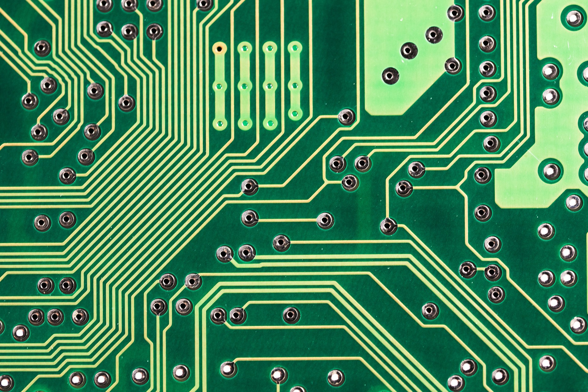
Widen the width of the power supply and ground cable. It is recommended that the ground cable be wider than the power cable. The relationship between the ground cable, power cable, and signal cable is as follows:
The PCB of digital circuit can be formed into a circuit of wide ground wires, that is, to form a ground network for use (the ground of analog circuit cannot be used in this way).
With a large area of copper layer for ground, in the printed board is not used in the place are connected with the ground as ground. Or multilayer board, power supply and ground wire each occupy a layer.

2. Common ground processing of digital circuit and analog circuit
Many PCBS are now no longer single-function circuits, but a mixture of digital and analog circuits. Therefore, it is necessary to consider the problem of interference between them when wiring, especially the noise interference on the ground wire.
The digital circuit has a high frequency and the analog circuit has a strong sensitivity. For the signal line, the high frequency signal line is far away from the sensitive analog circuit devices as far as possible. For the ground wire, the whole PCB has only one node to the outside world, so the problem of digital and analog common ground must be handled inside the PCB, while the digital ground and analog ground are actually separated inside the board. They are not connected to each other, only in the PCB and the outside connection interface (such as plug, etc.). There is a bit of short wiring between digital and analog (please note that there is only one connection point), and there is also a bit of different wiring on the PCB, depending on the system Settings.
3. Lay the signal cables on the power supply or ground
In the wiring of multilayer printed board, because there is not much left in the signal line layer, more layers will cause waste will also increase the production of a certain amount of work, the cost is increased accordingly, in order to solve this contradiction, you can consider wiring on the power supply or the stratum. The power layer should be considered first and the formation second. Because it's better to preserve the integrity of the formation.
4. Processing of connecting legs in large area conductors
In a large area of grounding and power supply, the legs of commonly used components are connected to it, and the treatment of the connecting legs needs comprehensive consideration. In terms of electrical performance, it is better to fully connect the pad of the component leg with the copper surface, but there are some bad risks in the welding assembly of the components (such as 1, welding requires a high-power heater. 2, easy to cause virtual solder joint. Therefore, taking into account the electrical performance and process needs, make a cross shaped welding pad, which can make the possibility of virtual welding spot greatly reduced due to excessive heat dissipation in the section during welding. The power supply of the multilayer plate and the treatment of the formation leg are the same.
5. The role of network system in wiring
In many CAD systems, the wiring is determined by the network system. Although the network is too dense, the path is increased, but the step is too small, the amount of data in the graph field is too large, which inevitably has higher requirements for the storage space of the equipment, but also has a great impact on the computing speed of the object computer electronic products. And some paths are invalid, such as those occupied by the welding pad of the component leg or those occupied by the installation hole, the grid is too sparse, and too few paths have a great impact on the rate of distribution. Therefore, it is necessary to have a reasonably dense grid system to support the wiring.
6. Design Rule Check (DRC)
After the wiring design is completed, it is necessary to carefully check whether the wiring design conforms to the rules formulated by the designer, and it is also necessary to confirm whether the rules formulated meet the requirements of the printed board production process. Generally, the following aspects are checked: line and line, line and component pad, line and hole, component pad and hole, the distance between hole and hole is reasonable, and whether it meets the production requirements.
Is the width of the power cord and ground wire appropriate? Is the coupling between the power supply and ground wire? Is there any place in the PCB where the ground wire can be widened?
Are optimal measures taken for critical signal lines (e.g., minimum length, protected lines, input and output lines clearly separated)
Whether the analog circuit and the digital circuit parts have separate ground wires.
Whether the graphics (such as ICONS, labels) added to the PCB will cause signal short circuit.
Whether the process line is added on the PCB, whether the solder resistance meets the requirements of the production process, whether the solder resistance size is appropriate, and whether the character marks whether the device pad is pressed.


Just upload Gerber files, BOM files and design files, and the KINGFORD team will provide a complete quotation within 24h.