1. Signal Layer: Signal layer
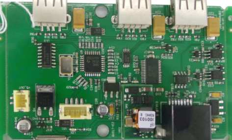
The signal layer is mainly used to arrange the wires on the circuit board; Including Top layer (top Layer), Bottom Layer (bottom signal layer) and Mid Layer (middle signal layer); Among them, the top signal layer is mainly used to place components, for the double layer board and multilayer board can be used for wiring; The bottom signal layer is mainly used for wiring and welding, sometimes can also place components; Intermediate signal layer used for distributing signal lines in multilayer panels.
2. Mechanical layer
It is commonly used to set the circuit board dimensions, data marks, alignment marks, assembly instructions, and other mechanical information.
3. Top/Bottem Overlayer (top/bottom silk screen layer)
esign for a variety of silk screen logo, such as component labels, characters, trademarks, etc. Generally, all kinds of annotation characters are in the top layer of screen printing.
4. Top/Button Paste (top/bottom paste)
It is used to correspond to the SMD (surface Mounted Device: surface mounted device) component solder joints when the welding furnace, the layer of negative output, so the plate on the display of the pad and hole on the circuit board to represent the solder paste on the area, that is, can be welded part.
5. Top/Botton Solder (top/bottom solder)
It is mainly used for laying solder resistance paint. This board adopts negative output, so the welding pad and hole part shown on the board represent the area on the circuit board without solder resistance paint, that is, the part that can be welded.
6. Keep-out Layer(No wiring layer)
Used to define the area on the board where components and wiring can be placed efficiently. Draw a closed area in this layer as the wiring effective area, outside the area is not automatic layout and wiring.
7. Internal Plane(Internal power layer)
It is usually called the internal electrical layer, including the power supply layer, the reference power layer and the ground plane signal layer. The internal power layer is output in negative form.
8. Drill Layer (Drill data layer)
The borehole layer provides borehole information and Drill drawing during circuit board manufacturing.
In the process of SMT patch processing in electronic factory, sometimes there will be a variety of bad tin conditions, affecting the molding effect of products. So how should we solve the problem when we encounter tin defects on SMT? The following Jingbang SMT patch factory Xiaobian for you to introduce the following:
First, the common preheating method in wave welding machine
1. Infrared heater heating;
2, air convection heating;
3, the method of combining hot air and radiation heating;
Second, wave soldering process curve analysis
1, wetting time: refers to the solder joint and solder contact after wetting start time;
2. Preheating temperature: preheating temperature refers to the temperature reached before PCB contacts with the crest surface;
3. Residence time: the time of a solder joint on PCB from the contact crest to the departure of the crest surface. The calculation method of residence/welding time is: residence/welding time = crest width/speed;
4, welding temperature: welding temperature is a very important welding parameter, usually higher than the solder melting point (183°C)50°C~60°C in most cases refers to the temperature of the solder furnace actual operation, the welded PCB solder joint temperature is lower than the furnace temperature, this is because of the PCB heat absorption results.

Three, prevent the occurrence of bridging
1, improve welding Ji activity;
2. Use weldable components /PCB;
3, improve the temperature of the solder;
4, improve the preheating temperature of PCB, increase the wetting performance of the pad;
5, remove harmful impurities, reduce the cohesion of the solder, in order to facilitate the separation of solder between the two solder joints.
The causes and protective measures of electrostatic discharge in SMT patch processing
In the manufacture of electronic products, electrostatic discharge will often damage the device, even make the device failure, resulting in serious losses, so electrostatic protection is very important in SMT production. The following Shenzhen Jingbang to introduce SMT patch processing and production of some electrostatic causes and protective measures.
1. Electrostatic Sensitive Device (SSD)
Devices that are sensitive to electrostatic reactions are called electrostatic sensitive components (SSDS). Electrostatic sensitive devices mainly refer to very large scale integrated circuits, especially metallized film semiconductor (MOS circuit). You can take different ESD preventive measures based on the SSD classification table.
2. Static power supply in the manufacture of electronic products
(1) Human body activities, friction, contact and separation between people and clothes, shoes, socks and other objects generated static electricity is one of the main static power sources in the manufacture of electronic products. Static electricity of human body is the main cause of hard (soft) breakdown of devices. The electrostatic voltage generated by human activities is about 0.5-2KV. In addition, the air humidity has a great impact on electrostatic voltage, if in a dry environment will rise 1 order of magnitude. When the human body is charged and touches the ground wire, it will produce a discharge phenomenon, and the human body will produce different degrees of electric shock response. The degree of response is called electric shock sensitivity.
(2) When working clothes made of chemical fiber or cotton are rubbed with working table and chair, the electrostatic voltage above 6000V can be generated on the clothing surface, and the human body is charged. At this time, when it is in contact with the device, it will cause discharge, which is easy to damage the device.
(3) Rubber or plastic sole insulation resistance up to 1013Ω, when friction with the ground to generate static electricity, and make the body charged.
(4) When resin, paint film and plastic film encapsulated devices are placed in packaging for transportation, the surface of devices and packaging materials friction can generate hundreds of volts of electrostatic voltage, discharge sensitive devices.
(5) With PP(polypropylene), PE(polyethylene), PS(polyvinyl vinyl), PVR(polyamine), PVC and polyester, resin and other polymer materials made of all kinds of packaging, material box, turnover box, PCB frame, etc., may produce 1-3.5KV electrostatic voltage due to friction, impact, discharge on sensitive parts.
(6) Ordinary working table, electrostatic generated by friction.
(7) Concrete, wax-polishing floor, rubber board and other insulating ground insulation resistance is high, the static charge on the human body is not easy to leak.


