
Professional PCB manufacturing and assembly
Building 6, Zone 3, Yuekang Road,Bao'an District, Shenzhen, China
+86-13410863085Mon.-Sat.08:00-20:00


Printed circuit board layout is much more than what it looks like. A successful PCB layout will allow its circuits to be physically arranged to achieve better electronic performance of the board while still being fully manufactured. This requires careful management of library components, CAD Settings and parameters, component placement, wiring, and power supply network (PDN) design. In addition, layout designers must ensure that their work is fully documented and that the final product is ready to be included in the main electronic system of their design.
This is a lot of work, especially for engineers unfamiliar with the PCB layout process. To help with this workflow, it is recommended to have a comprehensive set of board layout guidelines for reference. Industry and enterprise standards will dictate the details of the design, but layout guidelines are important to help engineers navigate the board development process from start to finish. Here are some basic PCB design layout guidelines that can be used to develop your own board development guidelines.
Before the layout begins
Before the layout process can begin, several tasks need to be handled to ensure a successful design, starting with the PCB encapsulation library to be used.
When building libraries for your PCB layout, it is important to use industry standards (such as IPC) or manufacturer specifications for package sizes and dimensions. However, individual, corporate, or technological needs may also determine some of the changes. For example, a package in an RF design may require a smaller pad size than a standard digital design. Here are some additional guidelines for building your own PCB component package:
Make sure that any library parts you build have acceptable pad pattern sizes that are spaced according to the standards for that part.
PCB packages need to contain all the necessary elements, such as part Outlines, silkscreen marks, and reference marks.
A good rule of thumb is to make sure your manufacturer can build the parts you are designing before submitting them to the final design.
Another option is to use PCB packaging from an external CAD library vendor. Parts manufacturers often pre-build their own components for your design system, and some tools have browsers to easily download these parts.
Circuit board outline and layer stack
Before starting the board layout, you need to work with a mechanical designer to get a good outline shape. Although the design's form factors can be changed later, any changes can force a substantial redesign of the circuit to accommodate the new shape. In addition, most CAD tools will accept data imported from mechanical design systems, making your life easier. However, even with the imported data, you still need to make sure that the board is outlined correctly and contains all the necessary CAD elements for your design, such as forbidden areas.
")
The board stacking should also be done before the layout begins. Again, these can be changed later, but the potential impact on existing circuits could disrupt your design schedule and budget. The board stacking should also be fine-tuned for your specific design to ensure that the correct layer configuration is provided for impedance control routing and other signal integrity requirements. It is also important to select the board material at this stage so that appropriate wire widths and other design calculations can be made based on the physical properties of the material. These characteristics include dielectric constant, insulation quality, moisture absorption rate and dissipation coefficient.
CAD parameters and Settings
It is not uncommon to find designers working with the default Settings that come with their CAD systems. However, most CAD systems provide the user with broad fan control over color, fill pattern, shading, and font size and width. You can also change the display of certain objects, place one design element over another, set the grid, and specify layout and wiring priorities. These Settings are designed to increase your productivity, and you can save time by taking the time up front to optimize the Settings.
Setting the display parameters of a CAD system is an important first step in PCB layout
Guidelines for placing PCB components
Once the CAD library, circuit board outline, and other setup tasks are complete, the design can begin to lay out. The first step in this process is to place the PCB component package on the board. Placing components on the board must meet three main requirements: circuit performance, manufacturability, and accessibility.
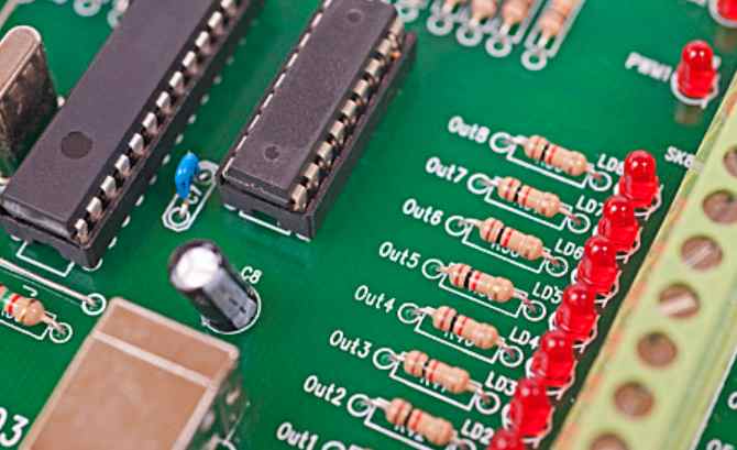
PWM in power supply design
May 09,2023


Just upload Gerber files, BOM files and design files, and the KINGFORD team will provide a complete quotation within 24h.