
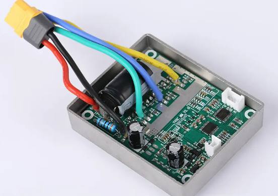
Professional PCB manufacturing and assembly
Building 6, Zone 3, Yuekang Road,Bao'an District, Shenzhen, China
+86-13410863085Mon.-Sat.08:00-20:00

Opening principle: Cut aniseed into small pieces according to the size required by MI
2. Inner layer: Paste dry film or printing oil, exposure and etching film inner layer anticorrosion detection is a process of graphic transfer, through the use of film negative, ink/dry film and other media under ultraviolet light, the line graphics required by the customer will be made on the inner layer substrate, and then the unnecessary copper foil etching away, finally made into the inner layer of conductive lines. Pre-treatment: grinding plate inner dry film inner etching inner test + coarse copper plate surface, in order to increase the adhesion of the board and film + clean the board, get rid of the dry film and copper foil covering ink and copper foil covering
3. Plate pressing process: Browning, plate lining, pressing, X-RAY punching, hole and gong edge
4. Drilling process: The role of drilling: to produce a conductive channel on the circuit board that allows the later process to complete the connection between the upper/lower or intermediate circuit layers

5 wet process: copper sedimentation - outer dry film - graphic plating or plate plating - outer layer - corrosion plate - outer layer - corrosion copper detection action: deposit a layer of conductive copper layer on the hole wall of the circuit board insulation, conduction and the connection of the inner line. Outer dry film: stick dry film exposure image plating or plate plating: Function: increase the copper thickness of the circuit board hole \ wire \ face, so as to meet customer requirements. Outer etching: film retreat: The use of strong alkali can make the dry film dissolution or peeling properties of the unwanted dry film from the surface peel or dissolve corrosion plate: the use of bivalence copper ammonium and ion oxidation to the unwanted copper from the plate corrosion tin: The nitric acid in the tin removal water is used to react with tin to remove the tin layer from the board to the outer layer inspection :AOI&VRS takes the PCB image by CCD scanning, compares it with CAM standard graphics by computer and processes the logic of the design specification, marks the bad spots on the circuit board and sends the coordinates of the bad spots to the VRS, and finally confirms the bad spots Location.
6. Wet film process: the main process stations include: printing a layer of photosensitive ink on the outer wire board surface that has been formed and curing it, so as to protect the outer layer and insulation of the circuit board; pre-treatment grinding board, ink printing, oven exposure and image printing, character printing
7. Surface treatment process: Mainly according to the requirements of customers, the copper surface of the circuit board is processed by a layer. The main processing processes are: spray tin: spray a layer of weldable tin surface on the copper surface using hot air welding process. Tin sinking: The use of chemical principles through chemical treatment to deposit tin on the surface of the board. Silking: The depositing of silver on a surface by chemical processes. Gold deposition: The use of chemical principles to deposit gold on a surface. Gold plating: Using the principle of electroplating, through the current and voltage control of gold plating on the surface. Anti-oxidation: The use of chemical principles of an anti-oxidation chemical coated on the surface
8. Molding process: Mainly according to the requirements of customers, a formed circuit board is processed into the size and shape required by customers.
9. Open short circuit test inspection: mainly to check the open circuit and short circuit inspection of the line, as well as the use of visual inspection board quality.
10. Packaging and shipment: the qualified boards will be packaged and finally shipped to customers.
Surfacemount technology (SMT) is a new generation of electronic assembly technology developed from hybrid integrated circuit technology. It is characterized by surface mounting of components and reflow welding technology. It has become a new generation of assembly technology for electronic products manufacturing.
The wide application of SMT promotes the miniaturization and multi-function of electronic products, and provides conditions for mass production and low defect rate production. SMT is surface assembly technology, which is a new generation of electronic assembly technology developed from hybrid integrated circuit technology.
The main components of the SMT production line are: surface assembly components, electric subgrade board, assembly design, assembly process;
The main production equipment includes printing machine, dispensing machine, paste machine, reflow welding furnace and wave welding machine. The equipment includes testing equipment, repair equipment, cleaning equipment, drying equipment and material storage equipment.
Four reasons for PCB board copper throwing
Mar 27,2023


Just upload Gerber files, BOM files and design files, and the KINGFORD team will provide a complete quotation within 24h.