
Professional PCB manufacturing and assembly
Building 6, Zone 3, Yuekang Road,Bao'an District, Shenzhen, China
+86-13410863085Mon.-Sat.08:00-20:00

With the rapid development of electronic information industry, electronic products are developing in the direction of miniaturization, functionalization, high performance and high reliability. From the general surface mounting technology (SMT) in the mid-1970s, to the high density interconnect surface mounting technology (HDI) in the 1990s, and the application of various new packaging technologies such as semiconductor packaging and IC packaging technology in recent years, electronic installation technology has been developing towards high density. At the same time, the development of high density interconnection technology promotes the development of PCB to high density. With the development of installation technology and PCB technology, the technology of copper-clad plate as PCB substrate material is also progressing.
Experts predict that the global electronic information industry will grow by 7.4 percent annually for the next 10 years, and that the global electronic information industry market will reach 3.4 trillion dollars by 2010, of which 1.2 trillion dollars will be spent on electronic machines, and 0.86 trillion dollars will be spent on communication equipment and computers, which account for more than 70 percent. It can be seen that the huge market for copper cladding as an electronic base material will not only continue to exist, but is growing at a growth rate of 15%. The relevant information released by the copper clad plate Industry Association shows that in the next five years, in order to adapt to the development trend of high density BGA technology and semiconductor packaging technology, the proportion of high performance thin shaped FR-4, high performance resin substrate will be more and more large.
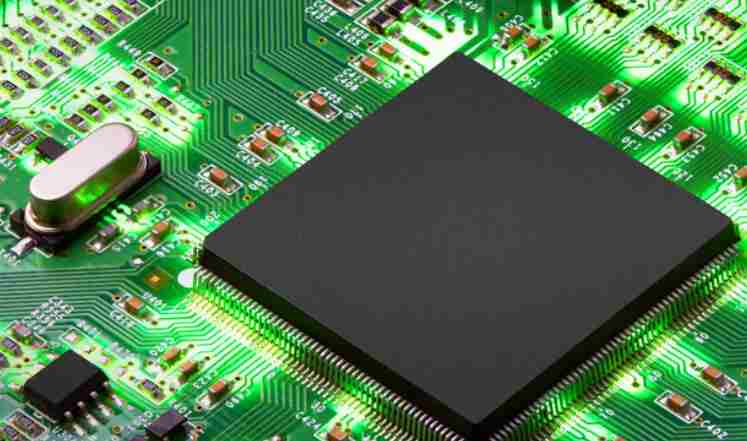
Copper clad plate (CCL), as the substrate material in PCB manufacturing, mainly plays the role of interconnection, insulation and support for PCB, and has a great impact on the transmission speed, energy loss and characteristic impedance of signals in the circuit. Therefore, the performance, quality, manufacturability, manufacturing level, manufacturing cost and long-term reliability and stability of PCB depend on the copper clad plate material to a large extent.
The technology and production of copper-clad plate have gone through a development course of more than half a century. Now the annual output of copper-clad plate has exceeded 300 million square meters worldwide. Copper-clad plate has become an important part of basic materials in electronic information products. Copper clad plate manufacturing industry is a sunrise industry, it is accompanied by the development of electronic information, communication industry, has a broad prospect, its manufacturing technology is a multi-disciplinary cross, mutual penetration, mutual promotion of high and new technology. The development of electronic information technology shows that copper clad technology is one of the key technologies to promote the rapid development of electronic industry.
The key task in the future development strategy of CCL industry, specifically in terms of products, should be made efforts in the five types of new PCB substrate materials, that is, through the development and technological breakthroughs in the five types of new substrate materials, to improve the cutting-edge technology of CCL. The development of the five new high performance CCL products listed below is the focus of the engineering and technical personnel of the copper clad industry in the future research and development.
A, lead-free compatible copper clad plate
At the European Union meeting of October 11, 2002, two "European directives" on environmental protection were approved. They will be fully implemented as of July 1, 2006. The two "European Directives" refer to the "Waste of Electrical and Electronic Products Directive "(WEEE) and the" Restriction Order on the Use of Certain Hazardous Substances "(RoHs). In these two statutory directives, it is clearly mentioned to prohibit the use of materials containing lead. Therefore, the development of lead-free copper cladding as soon as possible is the best way to deal with these two directives.
Two, high performance copper clad plate
The high performance copper clad plates referred to here include low dielectric constant (Dk) copper clad plates, copper clad plates for high frequency and high speed PCB, copper clad plates with high heat resistance, various substrate materials for lamination multilayer plates (resin-coated copper foil, organic resin film forming the insulation layer of lamination multilayer plates, glass fiber reinforced or other organic fiber reinforced semi-cured sheets, etc.). In the next few years (up to 2010), the corresponding performance targets should be achieved in the development of this type of high performance copper-clad sheet, based on the predicted future development of electronic installation technology.

Three, IC seal loading plate substrate material
It is a very important topic to develop the substrate material used for IC sealing loading plate (also known as IC packaging substrate). It is also an urgent need to develop IC packaging and microelectronic technology. With the development of IC packaging to high frequency, low energy consumption direction, IC packaging substrate in low dielectric constant, low dielectric loss factor, high thermal conductivity and other important performance will be improved. An important topic for future research and development is the thermal connection technology of substrate - effective thermal coordination and integration of heat escape etc.
In order to ensure the design freedom of IC packaging and the development of new IC packaging technology, it is necessary to carry out modeling tests and simulation tests. These two work, to master the characteristics of the substrate material for IC packaging, that is, to understand its electrical performance, heat and heat dissipation performance, reliability and other requirements, is very meaningful. In addition, further communication should be made with the IC packaging design industry to reach a consensus. The properties of the developed substrate materials are provided to the designer of the whole electronic products in time, so that the designer can establish accurate and advanced data basis.
PCB printing
Feb 11,2023


Just upload Gerber files, BOM files and design files, and the KINGFORD team will provide a complete quotation within 24h.