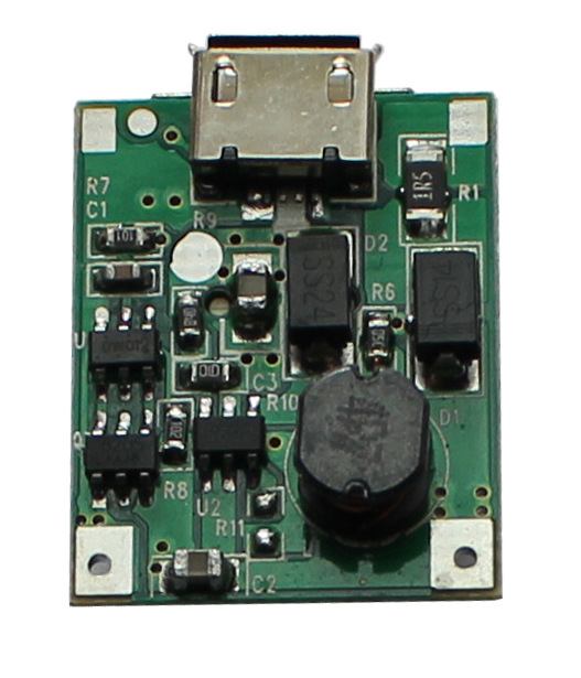
Chengdu Zicheng Electronics is a professional PCB designcompany engaged in electronic products circuit board design (layout and wiring design). Mainly undertake multi-layer, high density PCB design drawing board and circuit board design proofing business. Next, I would like to share with you the layout design of PCB.

Setting technique
Different design phases require different grid Settings, and the layout phase can use large grid points for device layout. For large devices such as IC and non-positioning connectors, grid accuracy of 50 to 100mil can be used for layout. For passive small devices such as resistors, capacitors, and inductors, grid accuracy of 25mil can be used for layout. The accuracy of large grid points is conducive to device alignment and beautiful layout.
Layout rule
1. Normally, all components should be arranged on the same side of the circuit board. Only if the top layer components are too dense, can some highly limited devices with low calorific value, such as patch resistance, patch capacitance, patch ic, etc., be placed on the lower layer.
2. On the premise of ensuring electrical performance, components should be placed on a grid, parallel or vertical arrangement, so as to be neat and beautiful. In general, components are not allowed to overlap; The arrangement of components should be compact and the components should be evenly distributed throughout the layout.
3. The minimum spacing between the adjacent pad shapes of different components on the circuit board should be greater than 1MM.
4. Generally, the distance from the edge of the circuit board is not less than 2MM. The best shape for a board is a rectangle with a 3:2 or 4:3 aspect ratio. When the size of the circuit board is larger than 200mm*150mm, the mechanical strength that the circuit board can withstand should be considered.
Layout technique
In the layout design of PCB, it is necessary to analyze the unit of the circuit board and carry out layout design according to its function. All components of the circuit shall be laid out in accordance with the following principles:
1. Arrange the position of each functional circuit unit according to the circuit flow, so that the layout is convenient for signal flow, and the signals keep the same direction as far as possible.
2. Take the core components of each functional unit as the center and arrange the layout around them. The components should be arranged evenly, completely and compact on the PCB to minimize and shorten the leads and connections between the components.
3. For circuits working at high frequency, distribution parameters between components should be considered. The general circuit should try to arrange the components in parallel, which is not only beautiful, but also easy to install and mass production.
Special components and layout design
In PCB, special components refer to the key components of the high frequency part, the core components of the circuit, the components susceptible to interference, high voltage components, high calorific value components, and some heterogeneous components. The positions of these special components need to be carefully analyzed to make the layout in line with the requirements of circuit function and production. Their improper placement can lead to circuit compatibility and signal integrity problems, resulting in PCB design failures.
When designing how to place special components, the first consideration is the size of the PCB. The PCB size is too large, the printed circuit is long, the impedance is increased, the anti-drying ability is decreased, and the cost is increased. Too small, heat dissipation is not good, adjacent lines are easy to be interfered. After determining the PCB size, determine the swing position of the special components. Finally, all the components of the circuit are laid out according to the functional unit. The location of special components should generally follow the following layout principles:
1. Shorten the connection between high-frequency components as much as possible to minimize their distribution parameters and electromagnetic interference between each other. Easily interfered components do not get too close, input and output as far apart as possible.
2. Some components or wires may have a high potential difference. The distance between them should be increased to avoid accidental short circuit caused by discharge. High pressure components should be placed as far as possible out of hand reach.
3. Parts weighing more than 15G can be fixed with brackets and then welded. Those heavy and hot components do not put on the circuit board, to be placed on the bottom plate of the main case, but also consider the heat dissipation. The heat sensitive element should be far away from the heating element.
4. It is used for the layout of adjustable components such as potentiometer, adjustable inductance coil, variable capacitor and micro switch. The structural requirements of the whole wrench shall be considered. Some commonly used switches should be placed within easy reach of the hand if the structure permits. The layout of the components should be balanced, dense, and not top-heavy.
The success of a product depends on its intrinsic quality. But to take into account the overall beauty, both are the perfect wrench, to become a successful product.
1. Place components that closely match the structure, such as power sockets, indicators, switches, and connectors.
2. Place special components, such as large components, heavy components, heating components, transformers, IC, etc.
3. Place small components.
Layout check
1. Whether the size of the circuit board is consistent with the processing size required by the drawing.
2. Check whether the layout of components is balanced, arranged neatly, and all components are arranged.
3. Whether there is conflict at all levels. Such as components, frames, and private printing requirements.
4. Whether common components are convenient to use. For example, switches, inserts, and components that need to be replaced frequently.
5. Whether the distance between the heat sensitive element and the heating element is reasonable.
6. Check whether the heat dissipation is good.
7. Whether line interference needs to be considered.


