
Professional PCB manufacturing and assembly
Building 6, Zone 3, Yuekang Road,Bao'an District, Shenzhen, China
+86-13410863085Mon.-Sat.08:00-20:00


What is a pcb? PCB is the abbreviation of . Printed circuit board or printed circuit board, simply referred to as printed circuit board, is one of the important components of the electronics industry. PCB is the support of electronic components and the carrier of electrical interconnection of electronic components. Because it is made by electronic printing, it is called a "printed" circuit board.
FPC is a kind of PCB. FPC is a high reliability and excellent flexible printed circuit board made from polyimide or polyester film. It has the characteristics of high wiring density, light weight, thin thickness and good bending.
The difference between PCB and FPC
PCB generally uses FR4 as the base material, also known as hard board, can not bend or flex; FPC generally uses PI as the base material, is a kind of flexible material, can bend, bend at will.
The FPC can withstand millions of dynamic bends without damaging the wire. According to the requirements of space layout can be arbitrarily moved and expanded to achieve three-dimensional assembly, to achieve the integration effect of component assembly and wiring, which is incomparable to other types of circuit boards. Advantages.
FPC is not only a flexible circuit board, but also an important design method for connecting 3D circuit structure. This structure can be combined with other electronic product designs to create a variety of different applications. For example, PCB circuit boards are generally flat. At present, the common space expansion scheme is to use slots and interface cards, but FPC as long as the design of switch can make a similar structure, the direction design is more flexible. Using a connecting FPC, two rigid plates can be connected to form a set of parallel circuit system, and can also be arbitrarily turned to adapt to different product shape design.
So that's what pcb is, what fpc is, and the definition and difference between PCB and FPC. I believe you have a certain understanding of PCB and FPC after reading.
1. Design standards for the shape and size of PCB pad:
1. Call PCB standard package library.
2, the minimum single side of the pad is not less than 0.25mm, the maximum diameter of the whole pad is not greater than 3 times the diameter of the component.
3. Try to ensure that the distance between the edges of the two pads is greater than 0.4mm.
4. Pads with aperture exceeding 1.2mm or pad diameter exceeding 3.0mm shall be designed as diamond or plum pads
5. In the case of dense wiring, oval and oval joint pad is recommended. The diameter or minimum width of single-side pad is 1.6mm; Double-sided weak-current circuit pad only needs to increase the aperture by 0.5mm. Too large pad will cause unnecessary continuous welding.
Two, PCB pad hole size standard:
The hole in the pad is generally not less than 0.6mm, because the hole smaller than 0.6mm is not easy to be processed during drilling. Usually, the diameter of the metal needle plus 0.2mm is used as the diameter of the hole in the pad. For example, when the metal pin diameter of the resistance is 0.5mm, the diameter of the hole in the pad corresponds to 0.7mm, and the diameter of the pad depends on the diameter of the hole.
Three, PCB welding pad reliability design points:
1, symmetry, in order to ensure the balance of molten solder surface tension, both ends of the pad must be symmetrical.
2. Pad spacing, too large or too small pad spacing will cause welding defects, so ensure that the end of the component or pin and pad distance is appropriate.
3. The remaining size of the pad, after the component ends or pins overlap the pad, must ensure that the solder joint can form a meniscus.
4. The width of the pad should be basically the same as the width of the component end or pin.
In recent years, with the development of electronics industry technology, we can notice an obvious trend is reflux welding technology. Traditional plugins can also be reflow soldering in principle, commonly known as through hole reflow welding. The advantage is that all solder joints can be completed at the same time, thus minimizing production costs. However, temperature sensitive components limit reflow applications, both plug-in and SMDS. So people turned their attention to selective welding.
introduction
Circuit board, circuit board, PCB board, selective welding. This will be a cost effective welding method for the remaining plug-ins, and it will be fully compatible with future lead-free welding.
By comparing with wave soldering, the characteristics of selective welding process can be understood. The most obvious difference between the two is that in wave soldering, the bottom half of the PCB is completely immersed in the liquid solder, whereas in selective welding, only some specific areas are in contact with the solder wave. Because PCB itself is a poor heat conduction medium, it will not be heated to melt solder joints and PCB areas of adjacent components during welding. Flux must be applied before welding. In contrast to wave soldering, the flux is only applied to the lower part of the PCB to be welded, not the entire PCB. In addition, selective welding is only applicable to plug-in welding. Selective welding is a new method. A thorough understanding of selective welding technology and equipment is necessary for successful welding.
Selective welding processes Typical selective welding processes include flux spraying, PCB preheating, dip welding, and drag welding.
technology
Flux coating process in selective welding, flux coating process plays an important role. The flux should be active enough to prevent bridging and prevent PCB oxidation during welding heating and at the end of welding. The flux spraying is carried by the X/Y manipulator, and the PCB is passed through the flux nozzle to spray the flux onto the PCB to be welded. Fluxes are available in single nozzle spray, microporous spray, synchronous multi-point/pattern spray. The most important thing in microwave peak selection after reflow welding is the accurate spraying of flux. Microjet does not contaminate areas outside the solder joint. The minimum flux spot pattern diameter for micro-dot spraying is greater than 2mm, so the flux placement accuracy on the PCB is ±0.5mm to ensure flux always covers the weld site. The tolerances for the sprayed flux are provided by the supplier. The technical specification shall specify the flux dosage. A 100% safe tolerance range is usually recommended.

The primary purpose of preheating during selective welding is not to reduce thermal stress, but to remove the solvent and pre-dried flux so that the flux has the correct viscosity before entering the welding wave. In the process of welding, the influence of heat brought by preheating on welding quality is not the key factor. The PCB material thickness, device package specifications and flux type determine the preheating temperature Settings. In selective welding, there are different theories about preheating: some process engineers believe that PCB should be preheated before flux; Another view is to weld directly without preheating. Users can arrange the selective welding process according to the specific situation.
Chengdu Zicheng Electronics is a professional engaged in: networking hardware development, PCB board copy, PCB design, chip decryption, PCB welding, PCBA, SMT processing and other complete electronic solution development one-stop service enterprises.
Correct PCB pad design can be corrected if a small amount of skew occurs during patch processing due to the surface tension of the molten solder during reflow soldering. However, if the PCB pad is not designed correctly, it is easy to have component position deviation and suspension bridge welding defects after reflow welding, even if the position is placed very much. Therefore, in the design of PCB, it is necessary to pay attention to the design of PCB pad.

PCB layout design
Feb 10,2023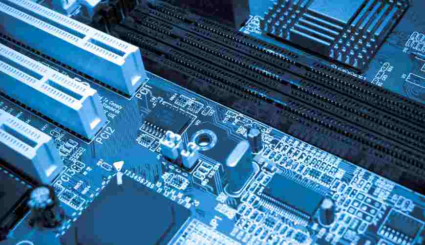


Just upload Gerber files, BOM files and design files, and the KINGFORD team will provide a complete quotation within 24h.