
Professional PCB manufacturing and assembly
Building 6, Zone 3, Yuekang Road,Bao'an District, Shenzhen, China
+86-13410863085Mon.-Sat.08:00-20:00

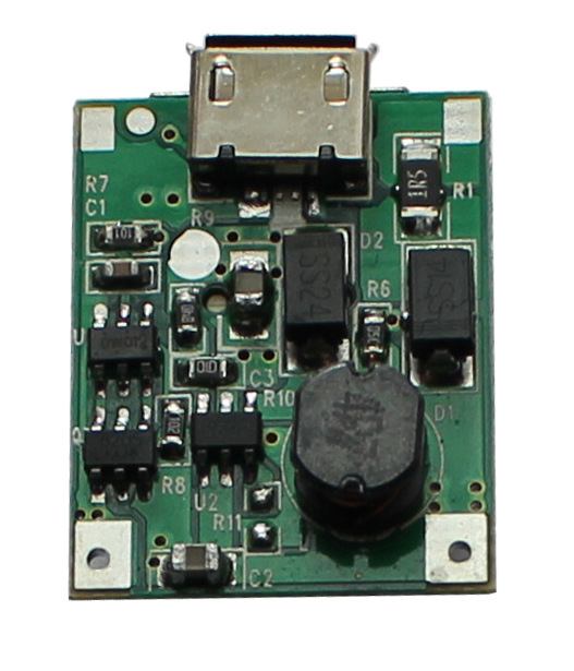
Printed circuit board (PCB) is a kind of information carrier integrating various electronic components. It is widely used in the field of electronics, and its quality directly affects the performance of products. It is hard to imagine electronic equipment without PCB, in the PCB manufacturing process, PCB components are generally using surface mount technology. With the development of electronic technology and electronic manufacturing, electronic products tend to be lighter, smaller and thinner. Therefore, the quality of PCB has a great influence on whether electronic products can work normally and reliably for a long time.
Firstly, PCB board defect detection includes solder spot defect detection and component detection. The traditional method of manual detection is easy to miss detection, slow detection speed, long detection time and high cost, which has gradually failed to meet the production demand. Therefore, it is of great practical significance to design an efficient and accurate machine vision PCB detection system equipped with industrial cameras to replace human eyes. Machine vision detection technology is built on the basis of image processing algorithm, through digital image processing and pattern recognition to achieve. Compared with the traditional manual detection technology, it improves the efficiency and accuracy of defect detection. To help PCB manufacturers detect defects at an early stage of production process implementation, more and more silk screen equipment manufacturers are integrating online machine vision technology into their silk screen equipment.
First, they can identify defects directly after the printing operation is implemented, and they can get operators to address relevant issues before major manufacturing costs are added to the PCB. This step typically includes when the circuit board is removed from the printing equipment, after it is cleaned in a cleaning agent, and when it is returned to the production line after repair.
In addition, as associated defects are discovered at this stage, defective boards can be prevented from reaching the back end of the production line. Therefore, the phenomenon of repair or scrapping formed in some occasions is prevented.
Perhaps most importantly, it gives the operator immediate feedback on whether the printing process is working well, thus effectively preventing defects.
In order to provide effective control during the process operation of this layer, an on-line visual system is configured to detect the condition of the pad on the PCB after tinning and whether the corresponding printing template gap is blocked or trailed. In most cases, the purpose of examining fine-spaced components is to optimize inspection time and focus on problem prone areas. For this reason, the time spent on testing is well worth it once possible problems have been ruled out. The second is the inspection of solder paste, which can be divided into two categories: inspection of solder paste on PCB and inspection of solder paste on printing template:
1. PCB inspection
Mainly detect printing area, printing offset and bridge phenomenon. The inspection of printing area refers to the area of solder paste on each pad. Too much solder paste may cause bridge, too small solder paste may also cause weak solder joint. The detection of printing offset is based on whether the solder paste on the pad is different from the specified position. The detection of bridging is to detect whether the amount of paste applied between two adjacent pads exceeds the specified amount. This excess paste may cause an electrical short circuit.
2, printing template detection
The detection of printing template is mainly to detect the phenomenon of blocking and trailing. Plugging detection refers to the detection of solder paste accumulation in the holes on the printing template. If the hole is blocked, then the solder paste applied at the next printing point may appear too little. The detection of trailing refers to whether there is excessive solder paste accumulation on the surface of the printed template. This excess paste can apply to areas of the board that should not be open, causing electrical connection problems.
In foreign countries, the application of machine vision is mainly reflected in the semiconductor and electronics industry, about 40-50% of which are concentrated in the semiconductor industry. Specific examples: PCB printed circuit: various production of printed circuit board assembly technology and equipment; Single-sided, double-sided, multilayer circuit board, copper-clad plate and required materials and auxiliary materials; Ancillary facilities and consumables, inks, potions and accessories; Electronic packaging technology and equipment; Screen printing equipment and screen surrounding materials.
In China, the application of visual technology began in the 1990s. Because the industry itself is an emerging field, coupled with the insufficient popularity of machine vision product technology, the application of the above industry is almost blank. At present, most domestic machine vision for foreign brands. Most domestic machine vision companies are basically from the agent of a variety of foreign machine vision brands started. With the continuous application of machine vision, the scale of the company is gradually growing, and the technology is gradually mature.


Just upload Gerber files, BOM files and design files, and the KINGFORD team will provide a complete quotation within 24h.