
Professional PCB manufacturing and assembly
Building 6, Zone 3, Yuekang Road,Bao'an District, Shenzhen, China
+86-13410863085Mon.-Sat.08:00-20:00

PCB copying board design and manufacturing is from the subtraction method to addition method, this paper mainly describes the PCB subtraction method and addition method related concepts and manufacturing process, for your reference to learn!
I. Introduction of PCB reduction process
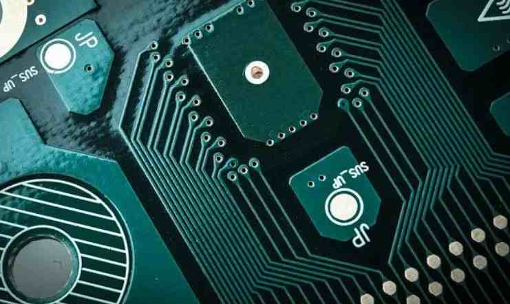
The reduction process is a conductive pattern obtained by selectively removing part of copper foil on the surface of copper clad laminate. The reduction method is the main method of manufacturing printed circuit, its biggest advantage is mature, stable and reliable process.
Printed circuits manufactured by the reduction process can be divided into the following two categories.
1. Non-perforated printed board (. Non -- plating -- thr 'ough -- hole Board)
This type of printed board is produced by screen printing and then etching out the printed board, or photochemical production. Non-perforated printed boards are mainly single panel, but also a small number of double panel, mainly used in television, radio. The following is the single panel production process:
Single clad copper foil substrate - photochemical/screen printing image transfer - removal of resist print - cleaning and drying - hole machining - shape machining - cleaning and drying - printed solder resistance paint - curing - printed marking symbol - curing - cleaning and drying - precoated flux - drying - finished product.
2. Plating -- through -- hole Board
On the copper coated foil laminate that has been drilled, the method such as electroless plating and electroplating should be adopted to make electrical connection between two layers or more than two layers of conductive graphics through electrical insulation. Such printed board is called perforated plated printed board. Perforated printed board is mainly used in computer, program control switch, mobile phone and so on. According to different electroplating methods, it can be divided into graphic electroplating and full plate electroplating.
(1) Graphic electroplating (Patter. n, P 'i 'n) on a double-sided copper clad laminate, using screen printing or photochemical method to form a conductive pattern, on the conductive pattern plated with lead tin, tin cerium, tin nickel or gold and other corrosion resistant metal, and then remove the corrosion inhibitor other than the circuit pattern, etching. The Pattern plating Process is also divided into the Pattern PlATIngAnd Etching Process and the Solder Mask OnBare Copper, SMOBC. The process of making double-sided printed boards with bare copper coated solder resistance film is as follows.
Double-sided copper foil plate raw material - punch positioning hole - CNC drilling - inspection - hair removal - electroless plating thin copper - electroplating thin copper - inspection - brush plate - film (or screen printing) - exposure development (or curing) - inspection repair - graphic plating copper - graphic plating tin lead alloy - film removal (or print removal) - Inspection repair - etching - lead tin - open test - cleaning - solder pattern - plug plating Nickel/gold one plug tape one hot air leveling one cleaning one screen printing mark symbol one shape processing one cleaning drying one inspection one packaging one finished product.
")
(2) Full plate plating (Panel, PNL) on the double sided copper clad laminate, plating
Copper to the specified thickness, and then screen printing or photochemical image transfer, to obtain the corrosion resistance of the positive phase circuit image, after corrosion and then remove the resist to make a printed board.
The whole plate electroplating method can be subdivided into plugging method and masking method. The process of making double-sided printed boards by masking (TenTIng) is as follows.
Double-sided copper foil plate bottom material one drill one hole metallization one whole plate plating thickening one surface treatment one pasting one photomasking type dry film one normal phase wire pattern one etching one film removal one plug plating one profile processing one inspection one printed solder resistance coating one solder coated hot air smoothing one printed mark symbol one finished product.
The advantages of the above method are simple process and good uniformity of coating thickness. The disadvantage is the waste of energy and the difficulty of manufacturing connectionless plate through hole printed board.
Ii. PCB addition process introduction
The method of selectively depositing conductive metal on the surface of insulating substrate to form conductive pattern is called addition method.
1. The advantages of addition method
Printed board using addition process manufacturing, its advantages are as follows:
(1) The addition method greatly reduces the production cost of printed boards because it avoids a large amount of etching copper and the resulting large amount of etching solution treatment costs.
(2) The process of addition method is about 1/3 less than that of subtraction method, which simplifies the production process and improves the production efficiency. In particular, the higher the product grade, the more complex the process of the vicious cycle.
(3) Addition process can achieve flush wire and flush surface, so as to manufacture SMT, high precision printed board.
(4) In addition process, due to the electroless copper plating on the hole wall and wire at the same time, the thickness of the copper plating layer on the hole wall and the conductive pattern on the plate surface is uniform, which improves the reliability of the metallized hole, and also meets the requirements of copper plating in the hole in the printed board with high thickness to diameter ratio.
2. Classification by addition method
The addition manufacturing process of printed boards can be divided into three categories:
(1) The Full Additive Process is the additive process which only uses chemical copper deposition to form conductive patterns. The CC - 4 method is taken as an example: drilling - imaging - adhesive treatment (negative phase) - electroless copper plating - removal of resist. Catalytic laminate is used as the substrate in this process.
(2) Semi-additive Process is used to chemically deposit metal on the surface of the insulating substrate, combined with electroplating etching or the combination of the three additive processes to form conductive patterns. The process flow is: drilling, catalytic treatment and adhesive treatment, electroless copper plating, imaging (electroplating resist), graphic copper plating (negative phase), removal of resist, differential etching. The base material used for manufacturing is common laminate.
(3) Partial Additive Process is used to manufacture printed boards on catalytic copper-coated laminates. Process flow: imaging (etching resistance) - etched copper (positive phase) - removal of resist layer - full plate coating electroplating resist - electroplating copper plating in a hole - removal of electroplating resist.


Just upload Gerber files, BOM files and design files, and the KINGFORD team will provide a complete quotation within 24h.