
Professional PCB manufacturing and assembly
Building 6, Zone 3, Yuekang Road,Bao'an District, Shenzhen, China
+86-13410863085Mon.-Sat.08:00-20:00


PCB copy boarddesign step one: PCB copy board board copy board advance work
1. Use schematic design tool to draw schematic diagram and generate corresponding network table. Of course, in some special cases, such as the circuit version is relatively simple, there is already a network table and so on, you can not carry out the schematic design, directly into the PCB design system, in the PCB design system, you can directly take parts packaging, manually generated network table.
2, manually change the network table will be some components of the fixed feet and other schematic diagram without the welding pad defined to the network connected with it, no physical connection can be defined to the ground or protection. The pin names of some devices with inconsistent names in schematic diagram and PCB package library are changed to be consistent with those in PCB package library, especially the two, triode, etc.
PCB copy board design step two: Draw your own definition of non-standard device package library
It is suggested to put the devices drawn by yourself into a dedicated design file of PCB library.
PCB copy board design step three: set up the PCB design environment and draw the printed circuit board with the middle of the hollowed out
1. The first step after entering the PCB copying system is to set up the PCB design environment, including setting the size and type of grid point, cursor type, version layer parameters, wiring parameters and so on. Most parameters can use the system default values, and these parameters after setting, in line with personal habits, do not need to change later.
2, planning the printed circuit board, mainly to determine the frame of the circuit board, including the size of the circuit version and so on. Place the appropriate size pad where the fixing holes need to be placed. For 3mm screws can be used 6.5~8mm outside diameter and 3.2~3.5mm inside diameter pad for standard board can be transferred from other board or PCB izard.
Note: Before drawing the board border, be sure to set the current layer as the Keep Out layer, that is, prohibit wiring layer.
Step 4 of PCB copy board design: Open all the required PCB copy board library files, call in the network table file and modify the parts package
This step is a very important link, the network table is the soul of PCB automatic wiring, is also the interface between schematic design and impression circuit plate design, only after loading the network table, the circuit plate wiring can be carried out.
During schematic design, ERC inspection does not involve the packaging of parts. Therefore, the package of parts may be forgotten during schematic design, and the package of parts can be modified or supplemented according to the design situation when the network table is introduced.
Of course, you can manually generate the network table directly within the PCB and specify the part package.
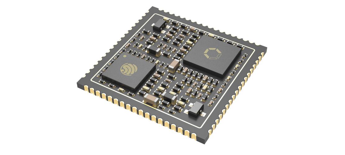
What is PCB board copy board?
What is a copy board? Copy board is also called cloning or imitation, is a product design of PCB board reverse technology research, copy board is equal to copy board, copy the circuit board on the hand, and then mass production. So how to copy the board, what do you need to prepare? Next by Chengdu Zicheng Electronic answer for you.
The first step is to take a PCBA circuit board and record the models, parameters and corresponding positions of all components on the pcba in notes or files. It is best to take a picture before the dissection, so as not to make mistakes during the recording process, especially the diode, the direction of the tertiary tube, the direction of the IC notch. There are a lot of BGA packages that we have to document as well.

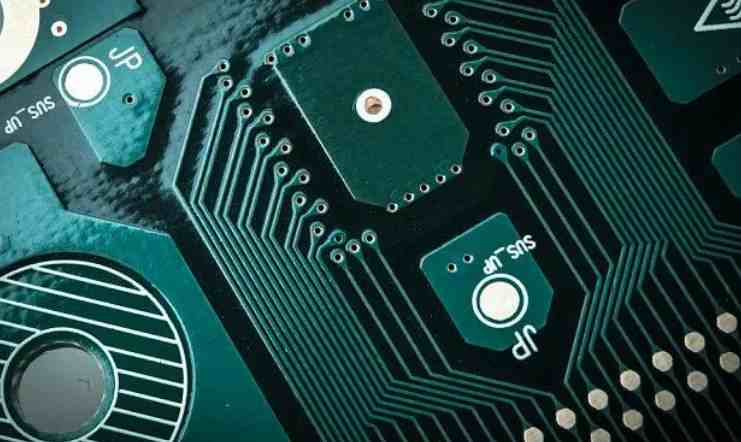
Second, after recording all the packaged components, remove all the components and remove the tin from the PAD hole. The PCBA circuit board is cleaned with industrial alcohol and placed in a scanner that is programmed to scan with slightly higher pixels so that a clearer image of each grain and circuit and structure can be seen. Then the top and bottom layers are lightly polished with gauze paper until the copper film shines, put them in the scanner, start photo shop, and sweep the two layers in color separately. Note that PCB must be placed horizontally and vertically in the scanner, otherwise the scanned image cannot be used.
The third step is to adjust the contrast and brightness of the canvas, so that the part with copper film is in strong contrast with the part without copper film, then turn the sub drawing to black and white, check whether the lines are clear, if not, repeat this step. If it is clear, save the picture as black and white BMP format files TOP.BMP and BOT.BMP. If there is any problem with the picture, you can use photo shop to repair and correct it.
The fourth step is to convert the two BMP files into protel files respectively, and transfer two layers into PROTEL. For example, the position of PAD that has passed two layers is basically identical with that of ⅥA, which indicates that the previous steps have been done well. If there is any deviation, repeat the third step.
Step 5, convert the BMP of the TOP layer to the TOP.PCB, be careful to convert to the SILK layer, which is the yellow layer. Then you trace the line on the TOP layer and place the device according to the drawing of step 2. Delete the SILK layer when you are done. Repeat until all layers are drawn.
In the sixth step, TOP.PCB and BOT.PCB are transferred into PROTEL, and it is OK to combine into a figure.
Step 7: Use a laser printer to print the to player and bottom layer onto the transparent film (1:1 ratio), place the film on the PCB, compare and see if it's wrong, if it's right, you're done.
A copy of the original board was created, but it was only half done. But also to test, test copy board electronic technology performance is the same as the original board. If it's one, it's really done.


Just upload Gerber files, BOM files and design files, and the KINGFORD team will provide a complete quotation within 24h.