
Professional PCB manufacturing and assembly
Building 6, Zone 3, Yuekang Road,Bao'an District, Shenzhen, China
+86-13410863085Mon.-Sat.08:00-20:00

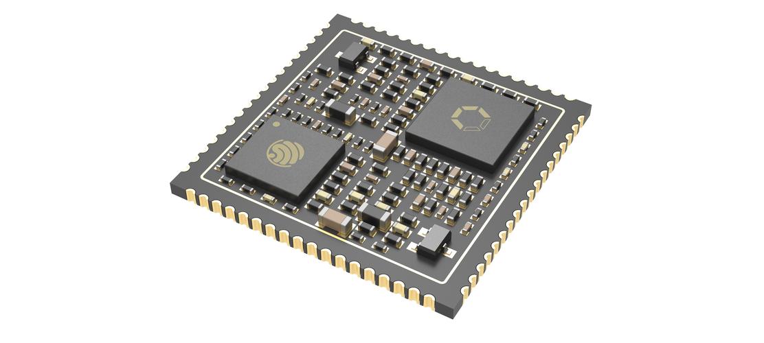
Simply put, a PCB is a PCB board with integrated circuits and other electronic components. It appears in almost every kind of electronic device and is the basis of the whole electronic product.
1. Misplaced characters
(1) The SMD solder of the character cover pad brings inconvenience to the conduction test of the printed board and the welding of components.
(2) The text design is too small, resulting in difficulties in silk screen printing, too large, resulting in overlapping text, difficult to distinguish.
2. Graphical layer abuse
(1) Made some useless wiring on some graphics layer. The original four-layer board was designed with more than five layers of wiring, causing misunderstanding.
(2) The design diagram saves trouble. Take Protel software as an example to draw all the lines of each layer with the Board layer, and use the Board layer to mark the line. In this way, when the optical data is drawn, the Board layer is not selected, so the connection is missed and short circuit. Or it can be short-circuited by the selection of board layer markers, thus maintaining the integrity and clarity of the graphic layer at design time.
(3) Against the conventional design, such as the design of the Bottom layer on the component surface and the design of the welding surface on the Top, causing inconvenience.
3. Overlap of pad
(1) The overlap of the pad (other than the surface-mounted pad) means the overlap of the hole. During the drilling process, the drill bit will be broken and the hole will be damaged.
(2) The two holes on the multilayer plate overlap. For example, one hole position is the isolation plate and the other hole is the connection plate (flower pad). In this way, the negative is shown as the isolation plate, resulting in scrap.
4. Set the aperture of single-side pad
(1) Single-side pad is generally not drilled, if drilling needs marking, the aperture should be designed to be zero. If the numerical values are designed, then the coordinates of the holes appear in this position when the borehole data is generated, there is a problem.
(2) Single side pad should be specially marked if there is drilling.
5. Paint the pad using filler blocks
Drawing pads with filler blocks can pass DRC inspection when PCB circuits are designed, but are not conducive to machining. Therefore, the pad cannot directly generate solder resistance data. When solder resistance is applied, the filler block area will be covered by solder resistance. Making it difficult to weld components.
6. Electrical ground is flower welding pad and wire
As the power supply is designed in the form of a flower pad, the grounding layer is contrary to the image on the actual printed board, and all connections are isolation lines. Designers should be well aware of this. By the way, care should be taken when drawing groups of power supplies or several types of ground isolation lines. Care should be taken not to leave gaps that short circuit the two groups of power supplies or cause the connection area to be blocked (separated from one group of power supplies).
7. The definition of processing level is not clearly defined
(1) Single panel design on the TOP layer. If front and back are not specified, the manufactured plate may not be easily soldered to the mounted assembly.
(2) For example, TOP mid1 and mid2bottom are used in a four-layer board design, but they are not placed in this order during processing, which needs to be explained.
8.PCB design has too many filler blocks or the filler blocks fill very thin lines
(1)gerber data is lost, and gerber data is incomplete.
(2) As the filling blocks are drawn line by line when processing optical drawing data, the amount of optical drawing data generated is quite large, which increases the difficulty of data processing.
9. Surface mount device pad is too short
This is for on-off testing. For too dense surface mount devices, the spacing between the two pins is very small, and the pad is very thin. To install the test pins, they must be staggered up and down (left and right). For example, if the pad is designed too short, it will not affect the installation of the device, but will make the test pins misaligned.
10. The spacing of large area grids is too small
The edges between the same lines that make up the large area grid lines are too small (less than 0.3mm). In the manufacturing process of printed board, after the image transfer is finished, it is easy to produce a lot of broken film attached to the board, resulting in broken lines.
11. Large area of copper foil is too close to the outer frame
Large area of copper foil and frame distance should be ensured at least 0.2mm above, because in the milling shape such as milling to copper foil, easy to cause copper foil warping and caused by its solder resistance off.
12. Shaped holes are too short
Length to width ratio of special-shaped hole ≥2:1, width > 1.0mm. Otherwise, it is easy to break the drill when the drilling machine processes special-shaped holes, causing processing difficulties and increasing costs.
13. Uneven graphic design
Pattern plating will cause uneven coating and affect the quality.
14. The design of the outline frame is not clear
Some customers have designed contour lines and these contour lines do not coincide, which makes it difficult for PCB manufacturers to judge which contour line should prevail.
PCB copy board four basic steps
Feb 09,2023


Just upload Gerber files, BOM files and design files, and the KINGFORD team will provide a complete quotation within 24h.