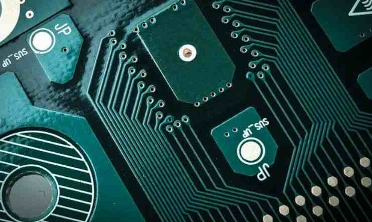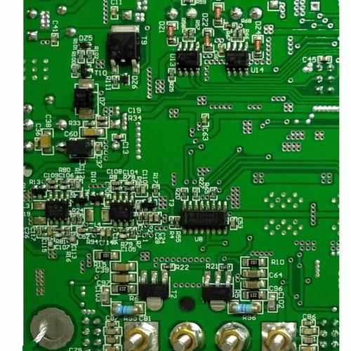
Because PCB copy board involves a copy board accuracy problem, for the mobile phone board and other precision requirements of the circuit board, we must copy out high precision PCB layout, so in the scanning process, we must carry out accurate numerical selection and setting of the scanner, but also need to ensure the accuracy of the original scanning image. Accurately speaking, the accuracy of the copy board is mainly determined by the original scanning accuracy.
In the process of PCB copying board, PCB scanning is undoubtedly the first step of all processes. Therefore, we first get a good PCB board, and then it must be scanned by the computer, and then backup the relevant parameters and the original PCB layout.
After the board is removed, the PCB light board is split, and we will officially enter the stage of copying the board, and the first thing we need to do is to scan, first of all, we need to store and record PCB images. It should be mentioned here that in order to better ensure the clear visibility of relevant parameters on PCB board after scanning, we must first remove the stains and residual tin on PCB board surface before scanning.

Here, we need to introduce the concept of DPI, where DPI means dots per inch. To be precise, the distance between every two points on the scanned image is 1000/DPI, in mil. In this way, when PCB is scanned in mobile phone board, DPI will be set as 1000, and the distance between two points on the image is 1000/1000=1mil, that is, the accuracy is 1mil at this time.
It should be noted that the higher the accuracy of the scan picture, the bigger the picture will be, and the higher the hardware requirements will be. Therefore, we need to set the DPI according to the specific situation of the original board, so as to ensure that the next steps of the copying board process can play the best effect.
What is Pcb screen printing?
The screen printing layer of PCB is the text layer. Its function is to formulate useful information on the PCB board, facilitate the installation and maintenance of the circuit, and print the required logo pattern and text code on the upper and lower surfaces of the PCB board, such as component number and nominal value, component contour shape and manufacturer's logo, production date, version, manufacturer and other information. It is also used to mark information such as component value, part number, polarity, etc. Screen printing can be letters, numbers, words.
Range of Pcb screen printing
When it comes to the whole process of screen printing process, it includes: safe production, use of equipment, required materials, process flow and control parameters, manufacturing process (principle, working conditions, screen preparation, making screen plates, ink mixing, use of ink scraper, positioning method of screen printing, plate inspection, brush, pre-drying, exposure, development, curing), document and process review, inspection and test items. It can be said that the range of PCB screen printing is very wide.
PCB silk screen printing rules
1. PCB should have complete relevant information of the manufacturer and anti-static label.
2. Screen printing characters follow the principle of "left-to-right" and "bottom-up" in the same direction.
3. The polarity of the polar element is marked on the screen, and the polarity direction will be easy to identify.
4. All components, mounting holes, and positioning holes have corresponding silkscreen labels. To facilitate the installation of the finished board, all components, mounting holes, and positioning holes are provided with silk labels. The mounting hole on the PCB is silkscreened with H1. , H2... Hn is used for identification.
5. The direction of the connector is marked on the screen.
6, PCB board name, date, version and other finished board information silkscreen position should be clear. Printed board name, date, version number and other printed board information on the PCB file should be clear and eye-catching.
7. There should be bar code position mark on PCB. If the PCB board space permits, there should be a 42*6 bar code screen frame on the PCB, and the bar code position should take into account that it can be easily scanned.
8. Whether the number of PCB light drawing files is correct, each layer should have the correct output, and there should be a complete layer output.
9. The component identifier on the PCB must be the same as that in the BOM.
10. There is no silk screen on the solder pad and tin path of the device to be tinned, and the number of the device shall not be blocked by the device after installation. (except for those with high density that do not require screen printing on PCB) In order to ensure the reliability of the welding of components, it is required that there is no screen printing on the welding pad of components; In order to ensure the continuity of the tin rail, no screen printing is required on the tin rail; In order to facilitate the insertion and maintenance of the device, the position number of the device after installation should not be blocked by the device after installation. Do not press the screen printing on the hole and pad, so as not to fall off the screen printing part when opening the solder resistance window, and the screen spacing is greater than 5mil.
The above is the introduction of PCB silkscreen printing. Chengdu Zicheng Electronic Equipment Co., Ltd. has focused on PCB industry for 13 years, and pays attention to us to gain more industry knowledge.


