
Professional PCB manufacturing and assembly
Building 6, Zone 3, Yuekang Road,Bao'an District, Shenzhen, China
+86-13410863085Mon.-Sat.08:00-20:00

We often see some Design principles of high frequency and high speed signals in textbooks or PCB Design Guide, including not to walk high speed signal lines on the edge of PCB circuit board. For the design antenna of board PCB, it is recommended that the antenna be as close to the edge as possible. What is scientific truth?
As we learned in junior high school, the Ampere Right hand rule says that the current in the wire travels in the direction of the thumb, and the magnetic field is generated on the wire. The direction of the magnetic field is the same as the direction of the finger of the right hand clenching the fist. The electric charge in the conductor will generate electric field. Electric field and magnetic field are a pair of good friends, collectively referred to as electromagnetic field.
According to Maxwell's theory of electromagnetic fields, a changing electric field produces a changing magnetic field in the space around it, and a changing magnetic field produces a changing electric field. In this way, the changing electric field and the changing magnetic field depend on each other, excite each other, produce alternately, and propagate through space with a certain speed from far to near, which is electromagnetic radiation. This has two diametrically opposed effects: On the positive side, all RF communications, wireless interconnection and induction applications benefit from the benefits of electromagnetic radiation; On the harmful side, electromagnetic radiation causes problems such as crosstalk and electromagnetic compatibility.
When the frequency of electromagnetic wave is low, it mainly propagates through the visible conductor. When the frequency gradually increases, electromagnetic waves will spill out of the conductor, and energy can be transferred outward without a medium, which is a kind of radiation. In low-frequency electric oscillation, the mutual change of magneto-electric is relatively slow, and almost all of its energy returns to the original circuit without energy radiation. However, in high-frequency electric oscillation, the magnetic and electric energy change with each other very fast, and the energy cannot return to the original oscillating circuit, so the electric energy and magnetic energy spread out of space in the form of electromagnetic wave, and have periodic changes. Electric and magnetic fields.
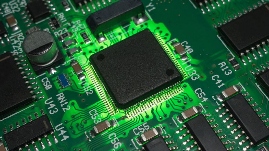
According to the above theory, each segment of wire passing through a high frequency current produces electromagnetic radiation, the intensity of which is proportional to the frequency. Some wires on PCB circuit board are used for signal transmission, such as DDR clock signal, LVDS differential signal transmission line, should not have too much electromagnetic radiation loss energy, cause interference to other circuits in the system; Some wires are used as antennas, such as PCB antennas, which want to convert as much energy as possible into electromagnetic waves and emit them.
For high speed signal transmission lines on PCBS (such as DDR clock signals, HDMILVDS high speed differential transmission lines), we have been looking for ways to minimize the radiation generated during signal transmission and the electromagnetic radiation generated by it. Signal transmission line has been summarized by experts some design principles, if the EMI of the signal transmission line is to be reduced, try to make the signal transmission line and the reference plane that forms the signal return path as close as possible. If the ratio between the width of the transmission line W and the spacing H of the reference plane is less than 1:3, the external radiation intensity of the microstrip transmission line can be significantly reduced.
For microstrip transmission lines, a wide and complete reference plane can also reduce the external radiation intensity of the electric field. The reference plane corresponding to the microstrip transmission line must be at least three times the width of the transmission line. The wider the reference plane, the better.
If the width of the reference plane is not large enough relative to the micro-single transmission line, the coupling between the electric field and the reference plane will be small and the external radiation of the electric field will increase significantly.
Therefore, in order to reduce the electromagnetic radiation of the high-speed signal transmission microstrip line, the reference plane corresponding to the microstrip transmission line should be as large as possible. If the high-speed microstrip transmission line runs parallel to the edge of the PCB board, relatively speaking, the coupling between the reference plane and the high-speed signal line becomes less, naturally resulting in a significant increase in the external radiation of the electric field.
Similarly, high speed IC and crystal oscillator should be placed away from the edge of the plate as far as possible. High speed ics also require a full and wide reference plane for electromagnetic coupling to reduce EMI.
For airborne antennas, we want to radiate as many electromagnetic waves as possible into space. Therefore, the design of vehicle antenna violates the design principle of high-speed transmission line. The onboard antenna needs to be placed at the edge of the board and where the antenna area is located. Copper foil planes need to be banned. Yes, copper foil exclusion zones need to be placed on all layers. And the antenna should be separated from the ground plane of the printed circuit board.

Procedures to be noted in SMT patch production
Feb 09,2023


Just upload Gerber files, BOM files and design files, and the KINGFORD team will provide a complete quotation within 24h.