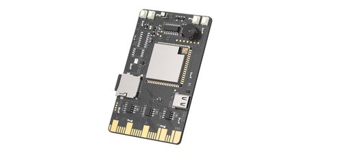
As far as the development and production process of multilayer PCB is concerned, there are often some product quality problems, especially the inner layer of multilayer PCB. With the development of higher density of electronic assembly, wiring density is higher and higher, and there are many inside and outside. Width and spacing 0.10-0.075mm, there are buried holes and blind holes between the small holes and microholes. Such as the ball grid array - a form of assembly structure. According to the requirements of the assembly structure, the PCB must be designed and manufactured to meet the design requirements of the outer wiring density of 0.10-0.125mm, the inner layer of 0.10-0.075mm, the hole diameter of 0.25-0.35mm and the fact that it is a six-layer board, which requires very precise alignment between the layers. But often due to process errors, the inner layer of multilayer PCB sometimes short-circuited. The inner short circuit is the biggest quality problem of multilayer PCB. This is because multi-layer PCB are difficult to repair if there is a short-circuit defect in the inner layer. If such defects are found after Denso, huge economic losses will be caused. Therefore, in order to solve the problem of inner short circuit of multilayer PCB, the main process factors of inner short circuit should be identified first, and then the corresponding process countermeasures can be taken.
First, the impact of raw materials on internal short circuit:
The dimensional stability of multilayer PCB material is the main factor affecting the positioning accuracy of the inner layer. The effect of the coefficient of thermal expansion of the substrate and copper foil on the inner layer of multilayer PCB must also be considered. From the physical property analysis of the substrate used, laminates contain polymers, whose main structure will change at a certain temperature, which is commonly known as the glass transition temperature Tg. The glass transition temperature is a unique property of many polymers, second only to the coefficient of thermal expansion, and is the most important property of laminates. In the comparative analysis of two commonly used materials, the glass transition temperatures of epoxy glass cloth laminate and polyimide are Tg120℃ and 230℃, respectively. When the temperature is below 150℃, the natural thermal expansion of epoxy glass cloth laminates is about 0.01in/in, while the natural thermal expansion of polyimide is only 0.001in/in.
From the relevant technical data, it can be seen that the thermal expansion coefficient of laminate in X and Y directions is between 12-16ppm/℃ for every increase of 1℃, and the thermal expansion coefficient in Z direction is between 100-200ppm /°C, which is greater than that in X and Y directions. An order of magnitude. However, during the test, it was found that when the temperature exceeded 100℃, the Z-axis expansion between the laminate and the hole body was inconsistent, and the difference became larger. The natural expansion rate of the electroplated through hole is lower than that of the surrounding laminate. Since the thermal expansion of the laminated body is faster than that of the porous body, this means that the through pore body is stretched in the direction of the deformation of the laminated body. This stress condition creates tensile stress in the through-hole body. As the temperature increases, the tensile stress will continue to increase. When the stress exceeds the breaking strength of the through-hole coating, the coating will crack. At the same time, the higher thermal expansion rate of the laminate significantly increases the stress on the inner conductor and pad, leading to the cracking of the conductor and pad, resulting in the short circuit of the inner layer of multilayer printed circuit board. Therefore, when manufacturing BGA and other high density packaging structures, we must carefully analyze the technical requirements of PCB raw materials, and the thermal expansion coefficient of the substrate and copper foil must basically match.

Two, film production and use error of internal short impact
The production of circuit graphics through the CAD/CAM system conversion, the final circuit image transmission ratio of 1:1. The diazo film for production is then generated by transfer method. There will be human and mechanical errors in the conversion process of the negatives used in plate making.After a period of development and statistical analysis of production data, it is often prone to the following deviations:
1. When positioning holes are played between layers, there will be deviations between layers due to visual errors.
2. Deviation caused by human and equipment when the light painting film is copied to the diazo film.
3. The displacement phenomenon generated during the image formation process of the film transfer circuit diagram leads to the deviation of the position of the imaging hole.
4. During the storage and use of the negative, due to the influence of temperature and humidity, the substrate of the negative expands and contracts, resulting in the deviation of the through-hole position of the negative.
5. Hole position deviation caused by human visual difference and positioning accuracy in the process of graphic transmission.
6. Deviation caused by the quality of the film itself.
These are the combined errors in PCB manufacturing process. According to military standards and international standards, the combined error value should not be greater than the width of the wire. If it exceeds the size range specified by standards and processes, it will cause short circuit in the inner layer of multilayer PCB. In order to ensure the quality of film production and the reliability of use quality, it is necessary to strengthen the monitoring and management of the process, so that the multi-layer PCB required for the manufacture of BGA structure devices must be correct, operable and efficient production, each process starts from the feed. Methods and strategies of sexual processes.
Three, the positioning system method accuracy affects the internal short circuit
Positioning must be carried out in the process of film forming, circuit pattern making, lamination, pressing and drilling. As for the type of positioning method used, it needs to be studied and analyzed carefully. These semi-finished products that need to be located will cause a series of technical problems due to the different positioning accuracy, and a slight mistake will cause short circuit in the inner layer of multi-layer PCB. The choice of positioning method should be based on the accuracy, applicability and effectiveness of the selected bits. There are many methods for the alignment between layers of multi-layer PCB, mainly including the following eight:
1. Pin positioning with two round holes.
2. Positioning with one hole and one slot.
3. Three-hole or four-hole positioning method.
4. Four-slot positioning.
5. Positioning method of MASS LAMINATE.
6. Locate and paste the locating mode.
7. Positioning mode after etching.
8. X-ray drilling positioning hole method.
As far as the eight process methods are concerned, the four-slot positioning process is suitable for the six-layer PCB positioning processing in terms of accuracy and reliability analysis. Of course, there are many factors affecting the positioning accuracy of multilayer PCB. The photopainting film, laminated core material, upper back plate and positioning equipment, production process equipment, process environmental conditions, process technology and the result of a variety of factors used in manufacturing. Due to the difference in positioning accuracy and the choice of process method, it is easy to cause the displacement of the inner layer of multi-layer PCB, resulting in the quality problem of the inner layer - short circuit.
Four. Influence of inner etching quality on inner short circuit
The inner etching process is prone to produce residual copper spots that have not been etched away. These copper residues are sometimes very small. Without visual inspection using an optical tester, it is difficult to see with the naked eye, and is carried to the lamination process, where residual copper is pressed into the inside of the multilayer PCB. Due to the high density of the inner layer, the remaining copper is most likely to lap between the two wires, causing a short circuit in the inner layer of the multilayer PCB.
FIve. Influence of laminating process parameters on internal short circuit
The inner plate must be positioned with dowel pins when laminating. If the pressure used when loading the plate is not uniform, the positioning hole of the inner plate will be deformed, and the shear stress and residual stress caused by too much pressure when pressing are also large. Layer upon layer shrinkage, deformation, etc., will lead to the short-circuit scrap of the inner layer of multi-layer PCB.
Six . Influence of drilling quality on internal short circuit
1. Analysis of hole position error
For high-quality, reliable electrical connections, the connection between the pad and the conductor should be maintained at least 50μm after drilling. To maintain such a small width, the positioning accuracy of the hole must be very high and the resulting error must be less than or equal to the technical requirements of the dimensional tolerances proposed by the process. But the error of the hole position is mainly determined by the precision of the drilling machine, the geometry of the drill bit, the characteristics of the cover and the backing plate and the technological parameters. The empirical analysis accumulated from the actual production process is caused by four aspects: the amplitude caused by the vibration of the drilling machine relative to the actual position of the hole, the deviation of the spindle, the sliding into the matrix caused by the point of the bit, and the impact caused by the bit entering the matrix. Resistance of glass fibers and bending deformation caused by cuttings. These factors will cause the hole position deviation and short circuit is possible.
2. According to the above deviation of hole position, in order to solve and eliminate the possibility of excessive error, it is recommended to adopt the multi-step drilling process, which can greatly reduce the impact of cuttings removal and the temperature rise of drill bit. Therefore, it is necessary to change the geometry of the bit (cross-sectional area, core thickness, taper, chute Angle, chute and long edge ratio, etc.) to increase the rigidity of the bit and improve the rigidity of the bit. The accuracy of hole position will be greatly improved. At the same time, the process parameters of the cover plate and drilling should be selected correctly to ensure that the precision of the drilling position is within the range specified in the process. In addition to the above guarantee conditions, external factors are also the focus of attention. If the inner layer is improperly positioned, drilling through hole offset, will also cause the inner layer open or short circuit.


