
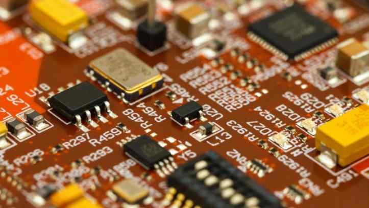
Professional PCB manufacturing and assembly
Building 6, Zone 3, Yuekang Road,Bao'an District, Shenzhen, China
+86-13410863085Mon.-Sat.08:00-20:00

Large PCB manufacturers use electroplating and etching processes to produce wiring on the board. For electroplating, the production process begins with the plating of copper over the outer plate substrate.
Photoresist etching is also used as another critical step in the production of printed circuit boards. The copper needed to protect during etching requires a balance between removing unwanted copper and keeping the resist in place. Protection is performed by coating the circuit pattern with a thin layer of resist (consisting mainly of a tin mixture), thus protecting the desired pattern from the etching agent.
Since etching removes excess copper from a clean blank plate, the thickness of the copper plus the coating cannot exceed the thickness of the photoresist. The subtraction process of first removing excess copper and then removing the resist produces the circuit pattern. Although manufacturers can use a bucket, tank, or spray machine to apply the etching agent, most selective high-pressure spray equipment can etch a standard-sized PCB design in less than a minute.
Although etchers or strippers are usually classified as ammonia etchers, the general ingredients usually include ammonia/ammonium chloride or ammonia/ammonium sulfate for spray etching. The resist prevents the etching solution from contacting the desired conductive pattern. Since the etching agent does not affect the resist, the unwanted copper is removed. PCB design outsourcing, professional things to professional people to do. Hefei MCU PCB design layout
Factors that may cause damage to flexible PCB boards. Hefei hybrid circuit PCB design quotation
PCB design industry specification content: for analog amplifying circuit, the coupling capacitor must be added between the connection of the near circuit and the amplifier circuit. For digital circuits, a packet is added with a decoupled capacitor. The filter capacitor should be installed as close as possible to the component to be filtered using a short shielded lead artificial coupling medium. All filtering must be masked and there must be isolation between input leads and output leads. The circuit with the characteristics of radiation source is installed in a metal box shielding, so that the interference is small. The pin of each IC should be added to the bypass capacitor and smooth capacitor to the ground. For low impedance noise sources, the filter should be high impedance, whereas for high impedance noise sources, the filter should be low impedance. Capacitor housing, auxiliary leading terminals, positive and negative terminals and circuit boards must be isolated. The filter connector must be well grounded. The metal shell filter uses surface grounding. The impedance matching between the HF current source and the destination must be satisfactory. The high frequency capacitor should be as close as possible to the power pin of the IC circuit and so on. Hefei hybrid circuit PCB design quotation

Shanghai Taofang Electronic Technology Co., LTD is located at Room 617, Building 41, No. 1969, Puxing Road. The company's business is divided into circuit board development, embedded development, Internet of Things solutions, software development, and so on. At present, we continue to innovate and improve services to provide customers with good products and services. The company will continue to enhance the key competitiveness of enterprises, strive to learn industry knowledge, comply with industry norms, rooted in the development of electrical and electrical industry. Taofang Electronics is based on the national market, relying on strong research and development strength, integration of cutting-edge technology concepts, quickly respond to the changing needs of customers.
PCB design latent circuit analysis
To ensure design reliability, latent circuit analysis provides a detailed path analysis for each identified path and applies component and path problems to all components in the path. This detailed analysis ensures that no latent paths exist. Another type of analysis is to ask questions about individual components when searching for latent indicators and latent labels. Digital latent analysis considers digital circuits and any design problems that can cause incorrect signal timing, switching, or mode errors.
When used in conjunction with circuit design, latent circuit analysis uses OrCAD to capture schematics and generate system netlists. In this way, latent circuit analysis can determine whether a bidirectional current path can be a latent path. The analysis is done by modeling all power switching components and all passive components. Instead of showing a model of an integrated circuit, the analysis shows how the IC has a switching circuit. This method relies on both functional positioning and design positioning.
Crosstalk in PCB design:
Where can I find crosstalk in a design, and what is an easy way to identify bad wiring in a PCB? You can use a full wave field solver, but you can use simpler analysis capabilities in your PCB design software to identify and prevent crosstalk.
Quite simply, crosstalk can occur between any two conductors carrying the signal in the PCB. This includes both digital and analog networks. When crosstalk occurs, a signal on one conductor couplings a part of itself to a new signal on a nearby conductor. Digital and analog signals may cause crosstalk in different ways.
Crosstalk is coupled to signal networks in two ways, depending on the main parasitic type that exists between two or more routes:
Capacitor crosstalk. This crosstalk occurs due to the wide-edge parasitic capacitance and the grounded coupling capacitance between the two conductors. The magnitude of capacitive crosstalk is proportional to the parasitic capacitance between the two conductors. For analog signals, the strength of capacitive coupled signals increases with frequency, so this crosstalk will dominate in high frequency networks or digital signals with very fast edge rates. Digital signals can cause transient ringing during and after switching, which can cause capacitive crosstalk.
Induced crosstalk. This type of crosstalk is caused by parasitic inductance between the two loops of the conductor. The magnitude of the induced crosstalk signal from the simulated attacker signal is proportional to the rate of current change in the attacker's trace. Digital signal will cause induction crosser in the switching process, during this period, the magnetic field from the signal will be in the damaged network in addition to PCB design, we provide professional PCB aging testing services, for your products escort.
Communication PCB design points for attention are as follows: 1, pay attention to the communication is half duplex or full duplex, 485 and Ethernet communication is to distinguish full duplex and half duplex; 2, clock, communication circuit design should pay special attention to the accuracy of the clock, otherwise clock confusion will cause communication errors; 3. The communication design should consider the length of the upper and lower edges. Oscilloscope must be used to measure whether the waveform is standard. 4, consider the communication distance, for example, 232 communication is better within 2 meters, 485 within 100 meters; 5, photoelectric isolation, this step is to prevent the interference of static electricity to the CPU when plugging; 6, current limiting, in the process of general RS232 communication, if the two sections of voltage is not the same, can consider adding a 100 ohm resistance; 7, filter circuit as close to the port as possible, magnetic bead or common mode electric feel terminal PCB line length should be small; If there are too many protective devices and the PCB cable distance between the magnetic bead and the terminal is large, add a Y capacitor or high voltage capacitor near the interface for filtering. The Y capacitor must meet the voltage resistance requirements. 8. If the EARTH can be grounded reliably (with metal shell grounding), then SGND is connected to the EARTH with a high-voltage capacitor. If the EARTH cannot be grounded reliably (floating), then SGND is directly connected to the EARTH short-circuited. Assembly type PCB component placement accuracy requirements. Hefei single chip microcomputer PCB design and development scheme
Cause of copper cable loss of PCB circuit board
Feb 08,2023


Just upload Gerber files, BOM files and design files, and the KINGFORD team will provide a complete quotation within 24h.