
Professional PCB manufacturing and assembly
Building 6, Zone 3, Yuekang Road,Bao'an District, Shenzhen, China
+86-13410863085Mon.-Sat.08:00-20:00

Understand PCB design hole inside pad
Although it is convenient for the designer to use holes in the pad of the circuit board, the process has many other advantages. In the meantime, there are a few things you should be aware of. Let's take a closer look at what a pad through-hole (VIP) design is and how it can help you when laying out printed circuit boards.
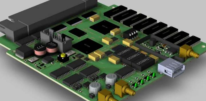
PCB design through hole
First let's look at the different types of through-holes:
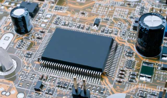
Through hole: This is the standard hole on almost every printed circuit board used to electrically connect the mesh from one layer to another. It's made with a mechanical drill and runs all the way through the circuit board.
Blind hole: can also be mechanically drilled. It starts in the outer layer and goes through the plate.
Buried hole: Similar to a blind hole, but it starts and stops on the inner layer.
Microvia: These through-holes are created with lasers and will * span two layers. Nail microholes are much smaller than conventional through mechanical drilling, making them more suitable for high-density circuit board designs.
However, designers need to pay attention to the cost of using holes. Just as the wiring on a circuit board generates inductance, so do the holes, which can affect the signal integrity of a high-frequency network. Therefore, there are many considerations in how holes are used in PCB design. However, perforations are critical to successfully routing the board. As the number of component pins increases, it becomes more and more difficult to find a way to route all the networks connected to these devices, and this is where pad technology really helps.
You need to understand the hole paste design PCB design PDN design guide. Hefei hybrid circuit PCB design quotation
PCBA cost-benefit analysis
The ability to accurately compare attributes and processes is an important part of PCBA development. During the design process, components are usually selected based on performance criteria for specific metrics provided on the data sheet. The manufacturing process (especially mass production) is judged by the ratio of usable plates to constructed plates (the yield). The usefulness of these assessments depends on the metrics used for comparison.
This simple but accurate description illustrates that there is no real limit to the existence of FOM. Its value or advantage lies in the availability of similar devices or systems. Common uses or types of FOM are listed below:
Quality factor types of electronic PCBA
Component parameter
One of the common uses of FOM is to compare the performance of components. This usually involves a simple equation with multiple parameters to define a new comparable metric.
Equipment parameter
It is also useful to create an FOM to compare the performance aspects of different devices. For example, the total power loss FOM can be determined to compare different device technologies.
System parameter
One of the common metrics for evaluating system quality is comparing the available output to the application input. For the PCBA manufacturing process, this FOM is the yield.
Determine electronic PCBA FOM Kingsoft high speed PCB design manufacturer to understand PCB design hole inside pad.

PCB layout tips make it easy to create component pads
Layout of PCB board. They want to open the PCB database and start placing the components and wiring network. The problem, however, is that if you don't spend a lot of time creating the component pad geometry, the board layout can go horribly wrong. Let's look at some of these issues and how to create good component sizes that are error-free for PCB designs.
Creating parts is a question of when to avoid
Sometimes, creating the geometry or overlay of component land is a task that doesn't get the attention it deserves. Footprints are often created on the run, assigned to people unfamiliar with requirements, or extracted from unverified or outdated sources. Instead, the generation of component placeholder area should be viewed as the basis for good PCB layout and built to strict specifications. The overall goal should be to populate the PCB library with good parts and not worry about correcting errors later. If appropriate action is not taken during the creation of the geometry of the parts land
In the PCB design, in order to make the high frequency circuit board design more reasonable, better anti-interference performance, we should consider the following aspects: (1) Reasonable selection of layers: When wiring high-frequency circuit boards in PCB design, the inner plane in the middle is used as the power and ground layer, which can play a shielding role, effectively reduce parasitic inductance, shorten the length of signal lines, and reduce the cross interference between signals. Generally, the noise of four-layer board is 20dB lower than that of two-layer board. (2) Wiring mode: When wiring the high-frequency circuit board in PCB design, the wiring must be turned at a 45° Angle, which can reduce the transmission of high-frequency signals and the coupling between them; (3) Line length: When wiring high-frequency circuit boards in PCB design, the shorter the line length, the better, and the shorter the parallel distance between two lines, the better; (4) Number of holes: when wiring high-frequency circuit boards in PCB design, the fewer holes, the better; (5) Interlayer wiring direction: When wiring high-frequency circuit boards in PCB design, the direction of interlayer wiring should be vertical, that is, the top layer is horizontal and the bottom layer is vertical, which can reduce the interference between signals; (6) Copper coating: when wiring high-frequency circuit boards in PCB design, adding grounded copper coating can reduce the interference between signals; (7) Ground cover: in the PCB design of high frequency circuit board wiring, the important signal line for ground cover processing, can improve the anti-interference ability of the signal, of course, can also be the interference source for ground processing, so that it can not interfere with other signals; (8) Signal line: When wiring the high-frequency circuit board in PCB design, the signal line should not be looped, and should be wired according to the Daisy chain mode; . The advantage of a large package library in PCB design.
Photoresist etching on PCB designs
Feb 08,2023


Just upload Gerber files, BOM files and design files, and the KINGFORD team will provide a complete quotation within 24h.