
Professional PCB manufacturing and assembly
Building 6, Zone 3, Yuekang Road,Bao'an District, Shenzhen, China
+86-13410863085Mon.-Sat.08:00-20:00

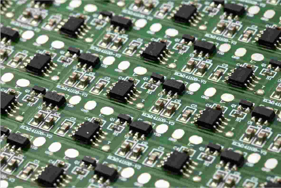
Long periods of slow change will lead to big changes. In the case of environmental protection increasingly loud voice, PCB surface treatment technology will definitely change in the future. Now there are many PCB surface treatment processes, the common five processes are hot air smoothing, organic coating, electroless nickel plating, gold dipping, silver dipping and tin dipping, which will be introduced one by one below.
1. Hot air leveling
Also known as hot air solder smoothing, it is the process of coating the PCB surface with molten tin lead solder and heating compressed air smoothing (blowing), so that it forms a coating layer that is resistant to copper oxidation and can provide good solderability. Hot air conditioning solder and copper at the joint of the formation of copper tin gold compounds. The solder protecting the copper surface is approximately 1 to 2mil thick. PCB for hot air polishing usually to soak in the molten solder; The air knife blows out the liquid solder before it sets; The air knife minimizes the meniscus of solder on the copper surface and prevents solder bridging. Hot air is divided into vertical type and horizontal type, horizontal type is generally considered to be better, mainly horizontal hot air leveling coating is more uniform, can realize automatic production. The general flow of hot air leveling process is: micro-etching → preheating → coating flux → tin-spraying → cleaning.

2. Organic coating process
Unlike other surface treatment processes, it acts as a barrier between copper and air; Organic coating is simple and inexpensive, which makes it widely used in the industry. The early organic coated molecules were imidazole and benzotriazole, which act as rust inhibitors. The latest molecules are mainly benzoidazole, which chemically bonds nitrogen functional groups to copper on printed circuit board. In the subsequent welding process, if only one layer of organic coating on the copper surface is not enough, there must be many layers. This is why liquid copper is often added to chemical tanks. After coating the first layer, the coating adsorbs copper; A second layer of organic coated molecules is then bonded to the copper until twenty or even hundreds of organic coated molecules have converged on the copper surface, thus guaranteeing repeated reflow soldering. The results show that the latest organic coating technology can maintain good performance in multiple lead-free welding processes. The general flow of organic coating process is: degreasing → micro-etching → pickling → pure water cleaning → organic coating → cleaning, and the process control is easier than other surface treatment processes.
3. Electroless nickel plating/gold leaching
Electroless nickel plating/gold dipping process is not as simple as organic coating. Electroless nickel plating/gold dipping process is like wearing thick armor to PCB; In addition, unlike organic coating as an anti-rust barrier, electroless nickel plating/gold leaching process can be useful in the long-term use of PCB circuit board and achieve good electrical properties. Therefore, electroless nickel plating/gold leaching is to coat the copper surface with a thick layer of good electrical nickel gold alloy, which can protect the PCB for a long time; In addition, it has environmental tolerance that other surface treatment processes do not have. Nickel plating is due to the diffusion of gold and copper, and the nickel layer can prevent the diffusion of gold and copper; Without the nickel layer, the gold would diffuse into the copper within hours. Another benefit of electroless nickel plating/gold leaching is the strength of nickel, with a thickness of only 5 microns limiting Z-direction expansion at high temperatures. Electroless nickel/gold plating also prevents copper from dissolving, which would benefit lead-free assembly. The general flow of electroless nickel plating/gold leaching process is: acid cleaning → micro-etching → preleaching → activation → electroless nickel plating → gold leaching. There are mainly 6 chemical tanks, involving nearly 100 chemicals, so the process control is difficult.
4. Silver dipping process
Between organic coating and electroless nickel plating/gold leaching, the process is simple and fast; It's not as complicated as electroless nickel/gold plating, nor is it a thick coat of armor for the PCB, but it still provides good electrical performance. Silver is the younger brother of gold, able to maintain good solderability even when exposed to heat, humidity and pollution, but tarnish. Silver immersion does not have the good physical strength of electroless nickel/gold plating because there is no nickel underneath the silver layer. In addition, silver immersion has good storage, after several years of assembly will not have a big problem. Silver immersion is a displacement reaction, it is almost submicron grade sterling silver coating. Sometimes the process of silver leaching also contains some organic matter, mainly to prevent silver corrosion and eliminate silver migration problems; This thin layer of organic matter is generally difficult to measure, and analysis suggests that the organism is less than 1% by weight.
5. Dip tin
Since all solder is currently based on tin, the tin layer can be matched to any type of solder. From this point of view, leaching tin process has a very promising development. However, tin whiskers appeared in the previous PCB board after leaching process. Tin whiskers and tin migration in the welding process will bring reliability problems, so the use of tin leaching process is limited. Later, organic additives were added to the leaching solution to make the tin layer structure granular structure, overcome the previous problems, but also has good thermal stability and weldability. Tin dipping process can form flat copper-tin intermetallic compounds, which makes tin dipping have the same good solderability as hot air leveling without the headache flat problem of hot air leveling. Tin immersion also does not have the diffusion problem of electroless nickel/gold plating - the copper-tin intermetallic compounds are able to bond firmly together. The tin dipping plate cannot be stored for too long, and must be assembled according to the order of dipping.
6. Other surface treatment processes
The application of other surface treatment processes is less, the following is the application of relatively more nickel gold plating and chemical palladium plating process. Nickel-gold plating is the ancestor of the PCB surface treatment process. It has been around since the appearance of printed circuit board and has slowly evolved into other methods. It is the PCB surfaceconductor is first coated with a layer of nickel and then coated with a layer of gold, nickel plating is mainly to prevent the diffusion between gold and copper. There are two types of electroplated nickel gold: soft gold plating (pure gold, the surface of gold does not look bright) and hard gold plating (smooth and hard surface, wear-resistant, containing cobalt and other elements, the surface of gold looks brighter). Soft gold is mainly used in chip packaging gold wire; Hard gold is mainly used for electrical interconnection in non-welded places. Because of the cost, the industry often uses image transfer for selective plating to reduce the use of gold. Selective electroplating continues to increase in the industry due to the difficulty in controlling the electroless nickel plating/gold leaching process. Under normal circumstances, welding will cause electroplating to become brittle, which will shorten the service life, so avoid welding on electroplating; However, electroless nickel plating/gold leaching rarely occurs because gold is very thin and uniform. The process of electroless palladium is similar to that of electroless nickel plating. The main process is to reduce palladium ions to palladium on the catalyzed surface by a reducing agent (such as sodium dihydrogen subphosphate). The newly formed palladium can be used as a catalyst to promote the reaction, and thus palladium coatings of any thickness can be obtained. The advantages of electroless palladium plating are good welding reliability, thermal stability and surface flatness.
How to improve the reliability of PCB equipment
Feb 05,2023


Just upload Gerber files, BOM files and design files, and the KINGFORD team will provide a complete quotation within 24h.