
Professional PCB manufacturing and assembly
Building 6, Zone 3, Yuekang Road,Bao'an District, Shenzhen, China
+86-13410863085Mon.-Sat.08:00-20:00

The research of BGA technology began in the 1960s and was first adopted by IBM, but it was not until the early 1990s that BGA really entered the stage of practical application. Due to the previous popular high-density pin devices similar to QFP packaging, the limitation of fine spacing is that the fine leads are easy to bend, brittle and easy to break, which requires high requirements for the common flatness and mounting precision between the leads. The following PCBA processing manufacturersto explain how to layout and wiring BGA devices and how to solve the relevant knowledge of PCBA welding problems.
1. How to solve the problem of PCBA virtual welding
What is PCBA virtual welding? That is, the surface looks like welding, but the actual interior is not through, or it is in an unstable state that may or may not be through. It is more difficult to find the problem, which is often said cold welding. Some of them do not solder the component foot and welding pad due to poor welding or less tin, and others are caused by oxidation or impurity of the component foot and welding pad, which is not easy to see by the naked eye. Generally, it is caused by oxidation or impurity at the welding point and poor welding temperature and improper method.
The essence is that there is an isolation layer between the solder and the pin, they are not completely in contact with each other, the naked eye generally can not see its state, but its electrical characteristics and no conduction or poor conduction. The circuit characteristics are affected. PCBA virtual welding is a common line fault, there are two kinds, one is in the production process of PCBA, due to improper production technology, the unstable state of intermittent failure; The other is that after long-term use of electrical appliances, some of the more serious heating parts, the welding spot at the welding foot is very easy to appear aging stripping phenomenon caused by. The components must be moisture-proof storage, the in-line devices can be slightly polished, in welding, you can use solder paste and flux, it is best to use reflow welding machine, manual welding to good technology. As long as the first welding is good, there will be no virtual welding phenomenon. "Electrical appliances after long-term use, some of the more serious heating parts, the welding spot at the welding foot is very easy to appear aging stripping phenomenon". This is a bad board base.
2. Methods to solve PCBA virtual welding:
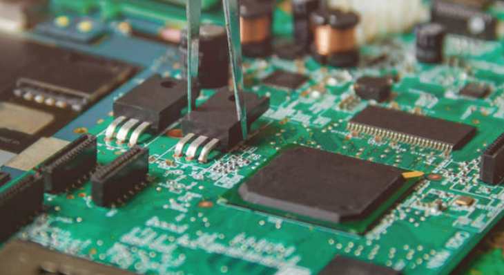
1) Determine the fault scope according to the fault symptom. 2) Appearance observation, focusing on large components and components with large calorific value. 3) Look through a magnifying glass. 4) Flip the circuit board. 5) Move the suspicious element by hand, and observe whether the pin solder joint is loose. Shenzhen Honglijie Electronics own PCB board factory and SMT patch factory, can provide PCB board manufacturing, component purchasing, DIP plug-in processing, SMT patch processing, PCBA function test one-stop service!
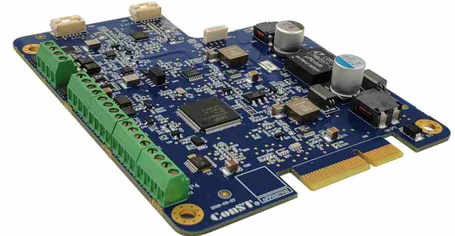
3. How to lay out and route BGA devices
KingFord has a professional PCB design team with excellent working experience, and can skillfully use various mainstream PCB design software. Next, we will introduce the layout and wiring skills of BGA devices in PCB design. With the rapid development of electronic products towards portable/miniaturized and networked direction, higher requirements are put forward for electronic assembly technology, among which BGA(Ball Grid Array Package) is a high-density assembly technology that has entered the practical stage. The research of BGA technology began in the 1960s and was first adopted by IBM, but it was not until the early 1990s that BGA really entered the stage of practical application. Due to the previous popular high-density pin devices similar to QFP packaging, the limitation of fine spacing is that the fine leads are easy to bend, brittle and easy to break, which requires high requirements for the common flatness and mounting precision between the leads. BGA technology adopts a brand new way of design thinking, which uses the structure of hiding round or column points under the package, with large lead spacing and short lead length. In this way, the BGA eliminates the defects of coflatness and warping due to lead problems in finely spaced devices. BGA is a commonly used component on PCB, usually 80% of high frequency signals and special signals will be pulled out from the Footprint of this type of packaging. Therefore, how to deal with the wiring of BGA devices will have a great impact on important signals. How is a typical BGA device routed? When wiring common BGA devices, the general steps are as follows:
1. Determine how many layers of plates are needed according to the number of BGA device pads, and carry out the laminated design.
2. Then fan out the main component BGA (that is, draw a small section of line from the pad, and then place a hole at the end of the line, and then pass the hole to the other layer).
3, and then from the hole escape wiring to the edge of the device, through the available layer to fan out, until all the pad escape wiring is completed. Fan out and escape wiring is carried out according to applicable design rules.

Including Fanout Control rule, RouTIng Width rule, RouTIng Via Style rule, RouTIng Layers rules and Electrical Clearance rules. If the rules are set unreasonable, such as the number of layers is not enough, the unlimited width is too wide to go out, the hole is too big to play the hole, the spacing violates the safety distance and so on, the fan will fail. When the fan out operation does not respond, please check your rule Settings and modify them as appropriate before fan out is successful. As shown in the picture below. The wiring color of each layer is different. The Fan Out dialog lets you control and define options for fan out and escape wiring, as well as options for blind holes (holes between Layer pairs, which can be set in the Layer Stack Manager dialog). Other options include whether to fan out two other rows at the same time as the internal rows, and whether only the pads to which the network is assigned are fanned out. How to wire very small BGA(0.4mm pitch) devices? Due to the complex processing technology of BGA, in addition to considering its functional design, the most important thing in the design stage is to communicate with PCB board manufacturers and patch assembly plants. Different manufacturers adopt different processes and have different capabilities. For processing and manufacturing costs, proofing and mass production are also different. Therefore, BGA design is more important to consider the processing cost, production rate and other factors.
The BGA I'm going to talk about today is not a fuel saver. This kind of BGA module design has been a refresh bottom line, belongs to the category of minimum processing capacity. Let's take a look at its parameter characteristics: BGA pad 0.3mm(12mil)BGA center spacing is 0.4mm(16mil) welding pad and edge to edge of the X and Y directions are 0.1mm(4mil). The welding pad and the welding pad edge are 0.27mm(10.8mil) along the diagonal direction. So here's the question! We review the post "How does Rule Setting Apply to My pcb Design? - -pcb manufacturing line width, line distance and aperture ", which has the introduction of the most precise machining capacity of PCB processing board factory. Now the main line width line distance and aperture limit processing capacity screenshots are as follows: here you watch attention! Minimum line width 0.1mm(4mil), minimum safety spacing 0.1mm(4mil), minimum laser aperture 0.1mm(4mil). We don't think about mechanical drilling, laser holes can not put!
PCB layer number identification skills
Feb 05,2023


Just upload Gerber files, BOM files and design files, and the KINGFORD team will provide a complete quotation within 24h.