
Professional PCB manufacturing and assembly
Building 6, Zone 3, Yuekang Road,Bao'an District, Shenzhen, China
+86-13410863085Mon.-Sat.08:00-20:00

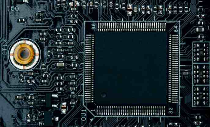
The substrate of the circuit board itself is made of an insulated, non-bendable material. The small wiring material visible on the surface is copper foil, which originally covers the entire circuit board and is etched away in the middle of the manufacturing process, leaving behind a network of tiny wiring. These wires, called wires or wiring, are used to provide circuit connections between the components on the board. Usually the color of PCB board is brown or green, which is the color of solder resistance paint. It's an insulating layer that protects the copper wire and prevents parts from being welded to the wrong place.
Now the graphics card and the motherboard are multilayer board, to a large extent can increase the area of wiring. More single or double-sided wiring boards are used for multilayer boards, and a layer of insulation is placed between each layer and pressed together. The number of layers of PCB board represents several independent wiring layers, usually the number of layers are even, and includes the outermost two layers, common PCB board is generally 4 ~ 8 layers of structure. Many PCB board layers can be seen by looking at the PCB board section. But the truth is, no one has such good eyes. So, let me show you one more way.
Multilayer circuit connection is through the buried hole and blind hole technology, motherboard and display card mostly use 4 layers of PCB board, but also some use 6, 8, or even 10 layers of PCB board. If you want to see how many layers of PCB, you can identify it by observing the pilot hole, because the four layers of board used on the motherboard and display card are the first and fourth layers of wiring, and the other several layers have other purposes (ground wire and power supply). So, as with the double board, the pilot hole will punch through the PCB board. If a pilot hole appears on the front of the PCB board but cannot be found on the back, then it must be a 6/8 board. If the same pilot hole can be found on both sides of the PCB board, it is a 4-layer board naturally.
Put the motherboard to the light, see the position of the pilot hole, if the light can be transmitted, this is 8/6 layers of board, or is four layers of board.
1. Process target
In PCB factories, the process of "packaging" is usually given less attention than other steps in the process, mainly because, of course, it does not produce added value, and because Taiwan manufacturers have long neglected to pay attention to the immeasurable benefits that packaging can bring. Japan has done this best. Careful observation of some household electronics, daily necessities, and even food in Japan, the same function, will make people prefer to spend more money to buy Japanese goods, which has nothing to do with worship of foreign beauty, but the mastery of consumer mentality. Therefore, packaging will be discussed independently, so as to let PCB manufacturers know that a small improvement may have a big effect. Another example is Flexible PCB, which is usually small and has a large quantity. The packaging method of Japan company may be specially made into a packaging container for the shape of a certain product, which is easy to use and protective.
2. Discussion on early packaging
For earlier packaging methods, see the table for outdated shipping packaging methods, with details of their deficiencies. There are still some small factories that use these methods to pack.
The domestic PCB production capacity is expanding rapidly, and most of them are exported, so the competition is very fierce. Not only the competition among the domestic factories, but also the competition with the top two PCB factories in the United States and Japan. In addition to the technical level and quality of the product itself are affirmed by the customers, the quality of the packaging must be satisfied with the customers. Almost some scale of the electronics factory, now will require PCB manufacturers shipped packaging, must pay attention to the following matters, some even directly to the shipping packaging specifications.
1. It must be vacuum-packed
2. The number of plates in each stack is limited according to the small size
3. The specifications of the tightness of each stack of PE film coating and the provisions of the width of the side
4. Specifications of PE film and Air Bubble Sheet
5. Carton weight specifications and others
6. Is there any special provision for cushioning before placing the board inside the carton
7. Specifications of resistance after sealing
8. Weight limit per case
At present domestic Vacuum Skin Packaging is much the same, the main difference is only the effective working area and the degree of automation.

Vacuum Skin Packaging 3, vacuum skin packaging
Operating procedure
A. Preparation: Position PE film, manually operate the mechanical action is normal, set PE film heating temperature, vacuum time, etc.
B. Stack plate: When the number of stacked plates is fixed, its height is also fixed. At this time, it is necessary to consider how to stack, which can make the maximum output and save the most materials.
a. The spacing of each stack of boards depends on the size (thickness) and (standard is 0.2m/m) of PE film, and the principle of heating becomes soft and elongated is used. At the same time of vacuuming, the covered board is stuck with bubble cloth. Its spacing is generally at least twice as thick as the total plate of each stack. Too big and waste materials; If it is too small, it is more difficult to cut and is very easy to fall off the adhesive or not adhesive at all.
b. The distance between the outermost plate and the edge shall be at least twice the thickness of the plate.
c. If the PANEL size is not large, according to the above packaging, it will waste materials and manpower. If the quantity is very large, can also be similar to the packaging of soft plate open mold container, and then do PE film shrink packaging. Another method, subject to the consent of the customer, is to leave no gaps between each stack of boards, but to separate them with cardboard and take the appropriate number of stacks. There are also hard paper or corrugated paper under.
C. Start: A. Press start, the heated PE film is lowered by the press frame and covers the table B. Then the bottom vacuum pump suction and close to the circuit board, and bubble cloth paste. C. Lift the outer frame after the heater is removed to cool it. D. Cut off the PE film and pull open the chassis to separate each stack
D. Packing: The packing method, if specified by the customer, must be in accordance with the customer's packing specification; If the customer does not specify, it is also necessary to establish the packing specification in the factory in order to protect the board from external damage in the transport process. Precautions, as mentioned above, especially the packing of exported products must be paid special attention to.
E. Other notes:
a. Information that must be written on the outside of the box, such as "mouth and wheat tip", material number (P/N), format, cycle, quantity, importance, etc. And "Made in Taiwan" (if exported).
b. Attach relevant quality certificates, such as slides, weldability reports, test records, and other dependent test reports required by the customer, and place them in the manner specified by the customer. Packing is not a question. If you do it carefully, you can save a lot of trouble that should not happen.v


Just upload Gerber files, BOM files and design files, and the KINGFORD team will provide a complete quotation within 24h.