
Professional PCB manufacturing and assembly
Building 6, Zone 3, Yuekang Road,Bao'an District, Shenzhen, China
+86-13410863085Mon.-Sat.08:00-20:00

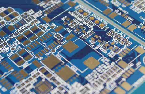
The cause of warping of the printed led circuit board, one aspect is that the substrate used (coppered plate) may warpage, but in the processing of the printed led circuit board, because of thermal stress, chemical factors, and improper production process will also cause the printed led circuit board to warpage.
The cause of warping of the printed led circuit board, one aspect is that the substrate used (coppered plate) may warpage, but in the processing of the printed led circuit board, because of thermal stress, chemical factors, and improper production process will also cause the printed circuit board to warpage.

Prevent warping of printed led circuit boards during processing
1, to prevent improper inventory caused or increased substrate warping
(1) As the copper clad sheet will increase warping due to hygroscopicity during storage, the hygroscopicity area of the single-sided copper clad sheet is very large. If the ambient humidity of the inventory is high, the warping of the single-sided copper clad sheet will be significantly increased. The moisture of the double-sided copper clad plate can only penetrate from the end face of the product, the moisture absorption area is small, and the warpage change is slow. Therefore, for the copper clad plate without moisture-proof packaging, pay attention to the warehouse conditions, minimize the humidity of the warehouse and avoid the bare copper clad plate to avoid the increased warping of the copper clad plate in storage
(2) Improper placement of copper clad plate will increase warping. If there is heavy weight on the vertical or copper clad plate, the good placement will increase the warping deformation of the copper clad plate
2, avoid due to printed led circuit board circuit design or improper processing process caused by warping, such as PCB board conductive circuit graphics imbalance or PCB board two sides of the line is obviously asymmetrical, one side there is a large area of copper, the formation of greater stress, so that the PCB board warping, High processing temperature or large thermal shock in the PCB process will cause the PCB board warping. For the impact caused by the improper inventory method of the cladding board, the PCB factory is better to solve, improve the storage environment and eliminate vertical placement, avoid heavy pressure. For PCB boards with large areas of copper skin in the line pattern, it is best to grid the copper foil to reduce stress
3. Eliminate substrate stress and reduce PCB warping during processing
Because in the PCB processing process, the substrate must be subjected to heat for many times and be subjected to a variety of chemical substances. For example, the substrate should be washed after etching, dried and heated, the electroplating of graphics is hot, the printing of green oil and the printing of identification characters should be heated and dried or baked with UV light, and the thermal impact of the substrate is also very large when the hot air is sprayed tin. These processes can cause the PCB to warp
4, wave soldering or dip welding, the solder temperature is high, the operation time is long, will also increase the substrate warping. For the improvement of the wave soldering process, the electronic assembly plant needs to cooperate because stress is the main cause of the substrate warping, if the copper clad plate is first baked (also known as the baking board) before the use of many PCB factories believe that this practice is conducive to reducing the warping of the PCB board.
The role of the drying board is to relax the stress of the substrate fully, which can reduce the warping deformation of the substrate in the PCB process
The method of baking board is: conditional PCB factory is to use a large oven baking board. Before putting into operation, a large stack of copper clad plates is sent into the oven, and the copper clad plates are baked for several hours to ten hours at a temperature near the glass transition temperature of the substrate. PCB board produced by copper-clad plate after baking plate, its warping deformation is relatively small, and the pass rate of the product is much higher. For some small PCB factories, if there is not such a large oven, the substrate can be cut small and then baked, but there should be heavy weights to press the board when baking the board, so that the substrate can maintain a flat state during the stress relaxation process. The temperature of the drying plate should not be too high, and the substrate will change color if the temperature is too high. It should not be too low, too low temperature takes a long time to relax the stress of the substrate.


Just upload Gerber files, BOM files and design files, and the KINGFORD team will provide a complete quotation within 24h.