Use the single-point or multi-point grounding method mentioned earlier to handle ground cables. Connect the analog ground, digital ground and high-power devices separately, and then converge to the ground point of the power supply. For high frequency and digital signals, both ends of the shielded cable should be grounded. For low frequency analog signals, single-ended grounding is generally used. Circuits that are very sensitive to noise and interference or circuits that are particularly serious with high frequency noise should be shielded by metal shields.
(8) Decoupling capacitance
The high frequency characteristic of decoupling capacitor is better in ceramic capacitor or multilayer ceramic capacitor. PCB board design, each integrated circuit between the power supply and ground to add a decoupling capacitor. The decoupling capacitor has two functions. On the one hand, it is the energy storage capacitor of the integrated circuit to provide and absorb the charging and discharging electric energy of the integrated circuit at the moment of opening and closing the door. On the other hand, it bypassed the high-frequency noise generated by the device. The typical decoupling capacitor in digital circuits is 0.1μF, and such a capacitor has a distributed inductance of 5nH, which can have a good decoupling effect on noise below 10MHz. Generally, a capacitor of 0.01 to 0.1μF can be selected.
Generally, it is required to add a 10μF charge-discharge capacitor to an IC of about 10 pieces. In addition, a capacitor of 10~100μF should be connected to the power supply and the four corners of the circuit board.
Seven, PCB board welding pad design requirements
Pad size: The inner hole size of the pad must be considered from the lead diameter and tolerance size of the component, as well as the thickness of the tin layer, aperture tolerance and the thickness of the metallized electroplating of the hole, etc. Normally, the diameter of the metal pin plus 0.2mm is used as the inner hole diameter of the pad. For example, if the metal pin diameter of the resistor is 0.5mm, the hole diameter of the pad should be 0.7mm, and the outside diameter of the pad should be 1.2mm plus the hole diameter of the pad, and the minimum should be 1.0mm plus the hole diameter of the pad. When the diameter of the pad is 1.5mm, the square pad can be used to increase the peeling strength of the pad. For pads with hole diameter less than 0.4mm, outer diameter of pads/hole diameter of pads =0.5~3. For a pad with a hole diameter greater than 2mm, the outer diameter of the pad/hole diameter of the pad =1.5~2.
Common pad size:
Pad hole diameter /mm
0.4; 0.5; 0.6; 0.8; 1.0; 1.2; 1.6; 2.0

Outer diameter of pad /mm
1.5; 1.5; 2.0; 2.0; 2.5; 3.0; 3.5; 4
Notes for the design of pad are as follows:
(1) The distance between the hole edge of the pad and the PCB board edge should be greater than 1mm, so as to avoid the defects of the pad during processing.
(2) welding pad fill tear drops, when the copper film line connected with the welding pad is thin, the connection between the welding pad and the copper film line should be designed into a tear drop, so that the welding pad is not easy to be peeled off, and the connection between the copper film line and the welding pad is not easy to disconnect.
(3) The adjacent pad should avoid having an acute Angle.
Eight, PCB board large area filling design
The purpose of filling a large area of PCB board has two purposes, one is heat dissipation, the other is to reduce interference with shielding, in order to avoid the heat generated during welding so that the gas generated by the circuit board has no place to discharge and the copper film off, should be filled in a large area of the window, the latter makes the filling grid. The use of copper coating can also achieve the purpose of anti-interference, and the copper coating can automatically bypass the pad and connect the ground wire.
Ix. PCB board crossover design
In the design of a single-sided PCB board, when some copper films cannot be connected, it is common practice to use jumper wires. The length of the jumper wires should be selected as follows: 6mm, 8mm and 10mm.
Ten, PCB board high frequency wiring design
In order to make the design of high frequency PCB board more reasonable, better anti-interference performance, PCB board design should be considered from the following aspects:
1. Reasonable selection of layers
Using the inner plane in the middle as the power supply and ground layer can play a shielding role, effectively reduce the parasitic inductance, shorten the length of signal lines, and reduce the cross interference between signals. Generally, the noise of the four-layer board is 20dB lower than that of the two-layer board.
2. Cable routing
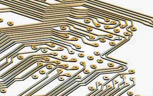
The line must be turned at a 45° Angle, which can reduce the transmission of high frequency signals and the coupling between them.
3. Cable length
The shorter the length of the wires, the shorter the parallel distance between the two wires, the better.
4. Number of holes
The fewer holes the better.
5. Wiring direction between layers
The wiring direction between layers should be vertical, that is, the top layer is horizontal and the bottom layer is vertical, which can reduce the interference between signals.
6. Apply copper
Adding grounded copper can reduce the interference between signals.
7. Cover the land
The important signal line for package processing, can significantly improve the anti-interference ability of the signal, of course, can also be the interference source for package processing, so that it can not interfere with other signals.
8. Signal cable
Signal routing cannot be a loop. Instead, route signals in Daisy chain mode.
9. Decoupling capacitance
Straddle the decoupling capacitor at the power end of the integrated circuit.
10. High frequency choke
Digital ground, analog ground, etc., to connect the common ground to a high frequency choke device, generally a high frequency ferrite magnetic bead with a wire through the center hole.


