
Professional PCB manufacturing and assembly
Building 6, Zone 3, Yuekang Road,Bao'an District, Shenzhen, China
+86-13410863085Mon.-Sat.08:00-20:00

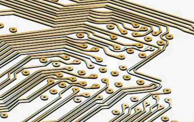
For the whole RF circuit, the RF units of different modules should be isolated with cavities, especially between sensitive circuits and intense radiation sources. In high-power multistage amplifiers, the isolation between stages should also be ensured. After the entire circuit tributary is placed, it is the processing of the shielding chamber. The processing of the shielding chamber has the following precautions:
The whole shielded cavity should be shaped as regularly as possible to facilitate casting. For each shielding cavity as far as possible to make rectangular, avoid square shielding cavity.
The perimeter of the shielded cavity is sealed, and the interface lines are generally introduced into the cavity by strip lines or microstrip lines, while the different modules inside the cavity adopt microstrip lines, and the connecting parts of different cavities are treated by grooves. The width of the grooves is 3mm, and the microstrip lines walk in the middle.
A 3mm metallized hole is placed at the corner of the cavity to fix the shield shell. Equal metallized holes should also be placed evenly on each long cavity to reinforce the supporting effect.
The cavity is generally windowed to facilitate welding of the shield shell. The thickness of the cavity is generally more than 2 mm, and 2 rows of Windows are added to the cavity. The holes are staggered to each other, and the spacing between the same row of holes is 150MIL.
Overshoot and undershoot: Overshoot is the first peak or valley value over the set voltage, for rising edge, refers to the highest voltage; For the falling edge, it is the lowest voltage. Undershoot is when the next valley or peak exceeds the set voltage. Excessive overshoot can cause the protection diode to work, leading to its premature failure. Excessive downstrokes can cause false clock or data errors (misoperation).
Oscillations and circumferential oscillations: Oscillations are recurring overshoots and downshoots. The oscillation of the signal is caused by the inductance and capacitance of the transition line, which belongs to the underdamped state, while the circumferential oscillation belongs to the overdamped state. Oscillations and circumferential oscillations, like reflections, are caused by a variety of factors and can be reduced by proper terminating, but cannot be completely eliminated.
Ground level rebound noise and reflux noise: When there is a large current inrush in the circuit, ground level rebound noise will be caused. For example, when a large number of chip outputs are turned on at the same time, a large transient current will flow through the power plane of the chip and the board. The inductance and resistance of the chip package and the power plane will cause power supply noise, which will produce voltage fluctuation and change on the real ground plane. This noise affects the actions of other components. The increase of load capacitance, the decrease of load resistance, the increase of ground inductance and the increase of the number of switching devices will lead to the increase of ground elastic.

Transmission channel electrical characteristics analysis
In multilayer PCB, most of the transmission lines are not only arranged on a single level, but staggered on multiple levels, and each level is connected through holes. Therefore, in multilayer PCB, a typical transmission channel mainly includes transmission line, line corner, through the hole 3 parts. At low frequencies, printed wire and threaded holes can be regarded as ordinary electrical connections connecting pins of different devices, which will not have much impact on signal quality. However, in the case of high frequency, printed lines, corners and holes should not only consider their connectivity, but also consider the effects of high frequency electrical characteristics and parasitic parameters.
Analysis of Electrical characteristics of transmission line in high speed PCB
In the design of high-speed PCB, it is inevitable to use a large number of signal connection lines, and the length is different. The delay time of signal passing through the connection line can not be ignored compared with the change time of the signal itself. The signal is transmitted on the connection line at the speed of electromagnetic wave, and the connection line is a complex network with resistance, capacitance and inductance. It needs to be described by the distributed parameter system model, namely the transmission line model.
A transmission line is used to transmit signals from one end to the other. It consists of two wires of a certain length, one is called the signal path and the other is called the return path. In low frequency circuits, the transmission line is characterized by pure resistance electrical characteristics. In high-speed PCB, with the increase of the transmission frequency of signal, the capacitive impedance between wires decreases and the inductive impedance on the wires increases, and the signal wire will no longer be presented as pure resistance, that is, the signal will not only be transmitted on the wire, but also in the medium between the conductors. If the signal frequency increases further, when > R, 1/(jωC)< For uniform conductors, without considering changes in the external environment, the resistance R, the parasitic inductance L of the transmission line, and the parasitic capacitance C are equally distributed (i.e. L1=L2=... =Ln; C1=C2=… =Cn+1).

Handle the ground
May 15,2023


Just upload Gerber files, BOM files and design files, and the KINGFORD team will provide a complete quotation within 24h.