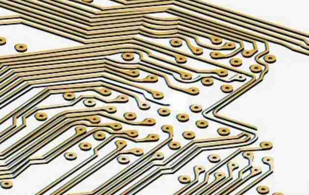
The FPC connector is used to connect the LCD display screen to the driver circuit (PCB). Currently, 0.4mm pitch products are the main products, and 0.3mm pitch products have also been widely used. With the recent trend of LCD drivers being integrated into LCD devices, the number of FPC pins will be reduced accordingly, and there are already related products on the market. In the longer term, it is expected that the FPC connector will be integrated into the framework of the phone or its LCD module along with other components of the phone.
Board to board connector
The development trend of mobile phone connectors is that the pin spacing and height are getting smaller and smaller. At present, the main pitch is 0.4mm, which will gradually develop to 0.35mm or even smaller, and the subsequent requirements are lower and have shielding effect. At the same time, the height of BTB(board to board connector) is gradually reduced to 0.9mm.
I/O connector
I/O connector is one of the most important access channels in mobile phone, including the connection of power supply and signal two parts, volume reduction and product standardization will be the main direction of future development. Nowadays, circular and MiniUSB connectors are commonly used. Micro USB connectors for mobile phones are gradually standardized under the promotion of European Union and GSM Association. At present, 5pin is the mainstream of the market. The Micro USB connector appears the development trend of combining standardization and customization. The mobile phone connector and the headphone connector used the same development trend. In 2012, MicroUSB will be mainly used as the standard charging interface in foreign countries. Further down the line, thinner connectors, visual effects and water resistance are required.
A transient protector is usually placed at the receiving end. Connect a short, thick wire (less than 5 times the width, preferably less than 3 times the width) to the chassis floor. The signal wire and ground wire from the connector are connected directly to the transient protector before being connected to the rest of the circuit.
A series of resistors and magnetic beads are usually placed at the receiving end, but for cable drivers that are vulnerable to ESD damage, a series of resistors or magnetic beads may also be considered at the driver end.
The filter capacitor should be placed at the connector or within 25mm of the receiving circuit.
(1) Use a short and thick wire to connect to the chassis or the receiving circuit (length less than 5 times the width, preferably less than 3 times the width).
(2) The signal wire and ground wire are first connected to the capacitor and then connected to the receiving circuit.
Make sure the signal line is as short as possible.
If the length of a signal cable is greater than 300mm, lay a ground cable in parallel.
Ensure that the loop area between the signal line and the corresponding loop is as small as possible. For long signal lines, the position of signal lines and ground lines should be changed every few centimeters to reduce the area of the loop.

Drive signals from a central location in the network into multiple receiving circuits.
Where possible, fill unused areas by connecting all layers of fill at 60mm intervals.
Make sure that the loop area between the power supply and the ground is as small as possible by placing a high-frequency capacitor near each power pin of the integrated circuit chip.
A high-frequency bypass capacitor is placed within 80mm of each connector.
Reset cables, interrupt signal cables, or edge trigger signal cables cannot be placed near the edge of the PCB.
Be sure to connect to the ground at the position of two opposite ends in any large ground fill area (approximately greater than 25mm×6mm).
When the length of an opening on the power supply or ground plane exceeds 8mm, connect the two sides of the opening with a narrow wire.
Connect the mounting holes to the circuit Commons or isolate them.
(1) When the metal bracket must be used with the metal shield device or case, a zero ohm resistor should be used to realize the connection.
(2) Determine the size of the mounting hole to realize the reliable installation of the metal or plastic support, the top and bottom of the mounting hole to use large welding pad, the bottom of the pad can not use solder resistance, and ensure that the bottom of the pad does not use wave soldering process for welding.
Protected signal cables and unprotected signal cables cannot be arranged in parallel.
Special attention should be paid to the wiring of reset, interrupt and control signal lines.
(1) High-frequency filtering should be adopted.
(2) Away from input and output circuits.
(3) Away from the edge of the circuit board.
The PCB should be inserted into the chassis. Do not install the PCB in the open position or inside joints.
Pay attention to the wiring of signal lines under the magnetic beads, between the pads and those that may come into contact with the magnetic beads. Some magnetic beads conduct electricity quite well and may produce unexpected conductive paths.
If a case or motherboard has several circuit boards, the most electrostatic sensitive circuit board should be placed in the middle.a


