
Professional PCB manufacturing and assembly
Building 6, Zone 3, Yuekang Road,Bao'an District, Shenzhen, China
+86-13410863085Mon.-Sat.08:00-20:00

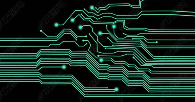
Printed circuit boards(PCBS) are an indispensable element in almost all electronic applications. They bring electronic and electromechanical devices to life by routing signals through circuits and fulfilling their functions. Many people know what PCBS are, but only a few know how they are made. Today, PCBS are constructed using a pattern plating process. They will move on to the next stage, which mainly involves etching and stripping. This article will effectively take you through the stages of the printed circuit board design process, but will focus more on the etching and stripping process of the board.
")
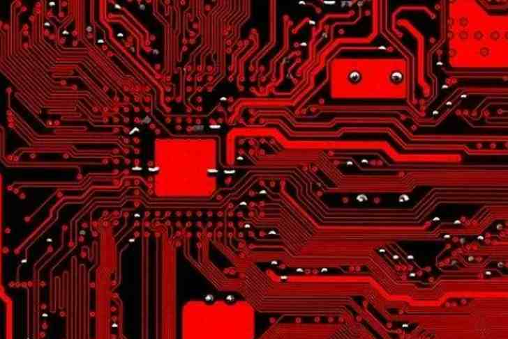
PCB design and manufacturing process
Depending on the manufacturer, the PCB manufacturing process may vary slightly, especially in terms of component installation techniques, testing methods, etc. They are mass-produced using a variety of automated machines used for drilling, electroplating, stamping and so on. Apart from some minor changes, the main stages involved in the PCB manufacturing process are the same.
Stage 1: An 8-step guide to etching PCBS
PCBS are made by gluing copper layers over the entire substrate. Sometimes both sides of the substrate are covered with copper layers. Performing a PCB etching process (also known as a controlled level process) uses a temporary mask to remove excess copper from the PCB panel. After the etching process, the circuit board is left with the required copper trace. PCB etching processes are performed using highly aggressive ammonia-based solutions ferric chloride or hydrochloric acid. Both chemicals are considered economical and abundant. To etch your PCB, you need to follow these steps:
1. Using any software of your choice, circuit board design is the initial stage of the etching process. When the design is ready, it is printed on transfer paper. Make sure the design fits the bright side of the paper.
2. Now, polish the copper sheet neatly, which will make the surface rough enough to accommodate the board design. There are a few things to keep in mind when performing this step:
(1) Use surgical or safety gloves when handling etching solutions, which will prevent oil from also transferring to the copper plate and hands.
(2) When sanding the copper sheet, ensure that all edges of the sheet are covered.
3. Clean the copper plate with water and alcohol. This will remove small copper particles from the surface of the plate. After cleaning, allow the board to dry completely.
4. Accurately cut out the PCB design and place the board face down on the copper plate. The plate is now passed through a laminator several times until it is heated.
5. After heating the plate, remove it from the laminator and place it in a cold bath. Stir the board for a moment so that the paper floats on the water.
6. Remove the circuit design from the slot and place it into the etching solution. Again, stir the board for half an hour, which will help dissolve the excess copper around the design.
7. Allow the board to dry once the excess copper has been washed off in the water bath. After the copper is completely dry, wipe the alcohol to wipe away the ink transferred to the board design.
8. You are now ready to etch the circuit board; However, you need to drill with the appropriate tools.
Stage 2: PCB stripping process
Even after the etching process, some copper remains on the board and is covered with tin/lead or electroplated tin. Nitric acid can effectively remove tin and keep the cracks in copper circuits below tin. In this way, you will have a clear copper outline on the circuit board, and the circuit board is ready to move on to the next process, flux resistance.
Stage 3: Flux resistance
This is an important part of the PCN design process, which uses a solder resistance material to cover the unsoldered areas of the board. As a result, it prevents solder from forming wires that create shortcuts to the leads of adjacent components.
Stage 4: PCB test
After the PCB is manufactured, testing is essential to check function and characteristics. In this method, the PCB manufacturer determines whether the board is working as expected. Today, PCBS are tested using a variety of advanced testing equipment. ATG tester is mainly used for testing large quantities of PCB, including flying needle and jig free tester.
Stage 5: PCB assembly
This is the final step in PCB manufacturing and mainly involves placing the various electronic components on their respective holes. This can be performed by either through-hole technique or surface mounting technique. A common aspect of both technologies is the use of molten metal solder to electrically and mechanically secure the leads of the components to the circuit board.
Brief introduction to the structure of one side flexible PCB
Single-side flexible PCB or single-side flexible PCB is the most basic type of flexible circuit. They consist of a flexible dielectric film laminated to a single sheet of copper. The copper layer is then chemically etched according to the specified circuit pattern design. Polyimide cladding can be added to the board for additional insulation and protection if desired.
Single-sided Flexible PCB: This design consists of a single conductive copper layer that can be bonded between two layers of insulation, or constructed from a polyimide insulation layer and uncovered sides. The inner copper layer then undergoes a chemical etching process to produce the circuit design. Single-sided flexible PCB board design supports the inclusion of components, connectors, pins and stiffener plates.
Single-sided Flexible PCBS with two channels: Some single-sided flexible PCBS have a two-channel design that allows you to access conductive materials from both sides of the circuit. This design feature requires flexible PCBS and dedicated layers in order to provide access to individual copper layers through the polyimide layer of the substrate.
As a connection device, the main benefit is that compared to traditional cables and rigid circuit boards, flexible circuits include:
Reduce wiring errors
Eliminate mechanical connector
Unparalleled design flexibility
Higher circuit density
More powerful operating temperature range
Stronger signal quality
Improved reliability and impedance control
Reduction in size and weight
Precautions for pcb splicing board
Feb 11,2023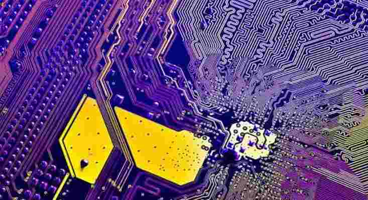


Just upload Gerber files, BOM files and design files, and the KINGFORD team will provide a complete quotation within 24h.