
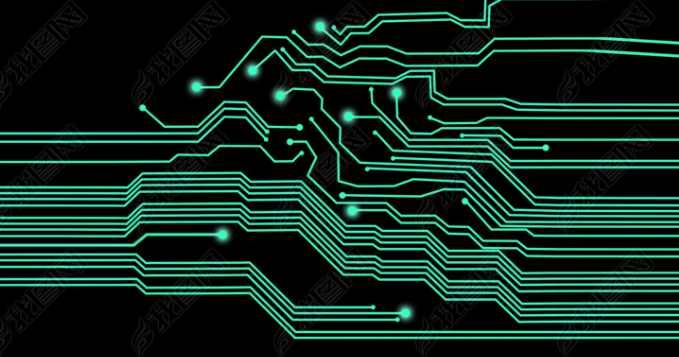
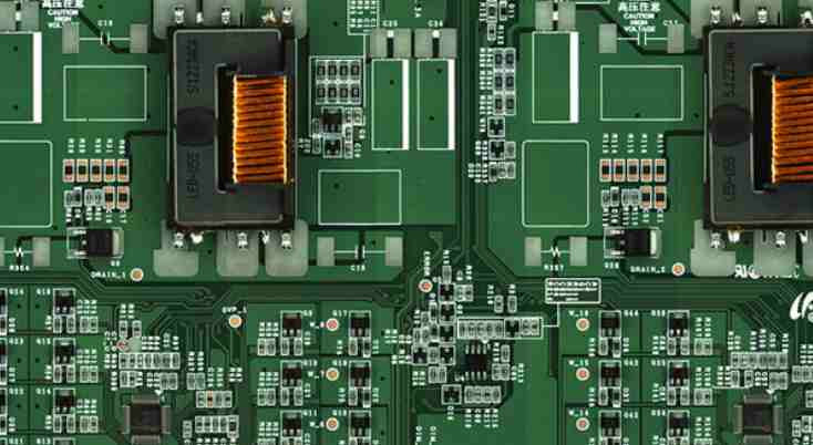
Professional PCB manufacturing and assembly
Building 6, Zone 3, Yuekang Road,Bao'an District, Shenzhen, China
+86-13410863085Mon.-Sat.08:00-20:00


The benefits of pcb Mosaic board
Some PCB size is too small to meet the requirements of SMT fixture, so it is necessary to assemble several PCBS to carry out patch production.
2. Cost savings
Some circuit board shape is special, different shape, through the board can be more effective use of PCB substrate area, reduce waste, save costs.

Precautions for pcb splicing board
1, PCB should pay attention to leave the edge and slot when assembling the board.
Leave the edge for later welding plug-in or patch can have a fixed place, slot is to split PCB board. The process requirements of leaving the edge are generally 2-4MM, and the components should be placed on PCB board according to the maximum width. Grooving is the forbidden wiring layer or material layer, which should be negotiated with PCB manufacturers for processing and marking by designers. PCB board is to facilitate production and improve work efficiency, you can choose by yourself.
2, v groove and groove are a way of milling outside.
It is easy to separate multiple boards when making the plate, so as to avoid damaging the circuit board when separating. Depending on the shape of the single variety you're putting together, the v-cut requires a straight line and is not suitable for four different sizes of boards.
3. Requirements for patchwork
Generally, there are no more than 4 kinds of plates. The number of layers, copper thickness and surface process requirements of each plate are the same. In addition, we will negotiate with the engineer of the manufacturer to reach the most reasonable version scheme.
The board is in order to save costs, if the production process is more complex, larger batch is recommended to produce alone, the board also bear the rejection rate of 10%-20%.
6 Keep out layer (Disable wiring layer)
Used to define the area on the board where components and wiring can be placed efficiently. Draw a closed area in this layer as the wiring effective area, outside the area is not automatic layout and wiring.
7. Silkscreen layer (Silkscreen Layer)
The screen printing layer is mainly used to place printed information, such as the outline and annotation of components, various annotation characters, etc. Protel 99 SE provides two silk-screen layers, Top Overlay and Bottom Overlay. Generally, all kinds of annotation characters are in the top screen printing layer, the bottom screen printing layer can be closed.
8 Multi layer
The solder plate on the circuit board and through the hole to penetrate the whole circuit board, and different conductive graphic layer to establish electrical connection relationship, so the system is specially set up an abstract layer - layer. Generally, the pad and the hole should be set on the multilayer, if the layer is closed, the pad and the hole can not be displayed.
9 Drill layer (Drill layer)
The borehole layer provides information about the boreholes in the circuit board manufacturing process (e.g., solder pads, which require boreholes). Protel 99 SE provides two Drill layers, Drillgride (drill indication drawing) and Drill drawing (drill drawing).
The distinction between solder resistance and solder aid
solder mask: solder mask, it refers to the part of the board to get green oil. Because it is a negative output, the part of solder mask is not solder oil, but silver-white.
paste mask: paste mask is used in machine patch and corresponds to the pad of all patch components. It is the same size as the toplayer/bottomlayer and is used to open steel mesh and leak tin.
Key points: Both layers are used for soldering on tin, not referring to a tin, a green oil; So is there a layer refers to the layer of green oil, as long as there is a layer on an area, it means that the area is insulated green oil? I haven't come across such a layer yet! The solder plate on the PCB board we painted will all solder layer by default. Therefore, the solder plate on the PCB board manufactured is coated with silver solder, and it is not surprising that there is no green oil. However, the wiring part on the PCB board we drew only has toplayer or bottomlayer layer, rather than solder layer, but the wiring part of the PCB board made is coated with green oil.
It can be understood in this way: 1. The solder resistance layer means that the window is opened on the green oil of the whole piece of solder resistance, in order to allow welding! 2. By default, green oil should be applied to areas without solder resistance layer! 3. paste mask layer is used for patch encapsulation! SMT packaging uses top layer, topsolder layer, and top paste layer. top layer is the same size as top paste, but topsolder is larger than them. The DIP package is used only for: topsolder and multilayer layer (after decomposition, I found that multilayer is actually toplayer, bottomlayer, topsolder, bottomsolder layer overlapping), topsolder/bottomsolder is larger than toplayer/bottomlayer.


Just upload Gerber files, BOM files and design files, and the KINGFORD team will provide a complete quotation within 24h.