
Professional PCB manufacturing and assembly
Building 6, Zone 3, Yuekang Road,Bao'an District, Shenzhen, China
+86-13410863085Mon.-Sat.08:00-20:00


What are PCB positioning holes
PCB positioning hole refers to the specific location of PCB hole in the PCB design process, is a very important link in the PCB design process. The function of the positioning hole is the machining benchmark of the printed circuit board. The positioning methods of PCB positioning holes are various, mainly according to the different accuracy requirements. Positioning holes on printed circuit boards should be represented by special graphic symbols. When the requirements are not high, the printed circuit board can also be used in the larger assembly hole instead.

In order to facilitate the PCB drilling and milling of the appearance of the fixed board, as well as the convenience of online testing, many circuit board manufacturers want users to design three nonmetallic holes on the PCB, positioning holes are usually designed to be nonmetallic holes, drilling diameter of mm or. If the Smmo is tight, at least two positioning holes must be placed diagonally. If the board is made, the board can also be regarded as a PCB, the whole board as long as there are three positioning holes. If the user does not place it, the circuit board manufacturer will automatically add it without affecting the circuit, or use the existing nonmetallic holes in the board as positioning holes.
Positioning method of positioning hole
Device Orifice interface devices and connectors are mostly cartridge components. The through hole diameter of the cartridge device is larger than the pin diameter of 8 ~ 20mil, good tin penetration during welding. It should be noted that there is an error in the aperture of the circuit board factory, the approximate error is ±0.05mm, each interval of 0.05mm is a kind of drill, the diameter of 3.20mm above, each interval of 0.lmm is a kind of drill. Therefore, when designing the device aperture, the unit should be converted into millimeters, and the aperture should be designed as an integer multiple of 0.05. The plate manufacturer sets the size of the drilling tool according to the drilling data provided by the user. The size of the drilling tool is usually 0.1 ~ 0.15 larger than the forming hole required by the user. The design aperture should be large rather than small, and the tolerance requirements should also be large rather than small. If it is crimped device, aperture should not increase, according to the data suggested design, and in the board description to explain what is crimped device, so that the circuit board manufacturers can try to control the error in the process of making the board, to avoid some unnecessary trouble.
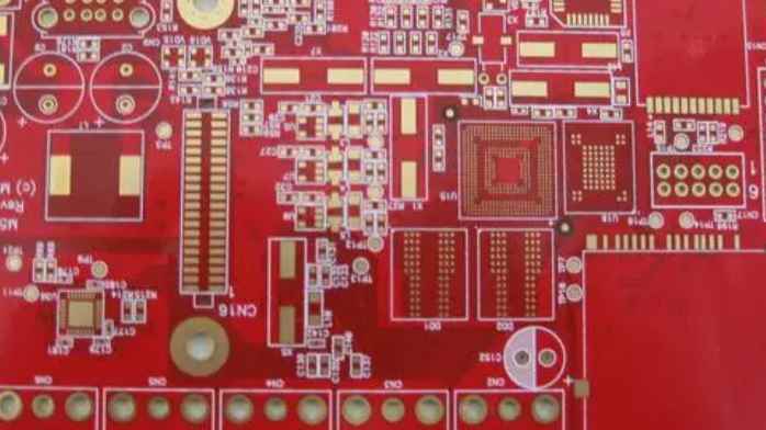
Boreholes are divided into metallized holes and nonmetallic holes. There is copper in the wall of the metallized hole, which can conduct electricity and is represented by PTH. There is no copper in the wall of the nonmetallic hole, so it cannot conduct electricity, which is represented by NPTH. The difference between the outside diameter and the inside diameter of the metallized hole diameter should be greater than 20mil, otherwise the welding ring of the pad is too small for processing and is not conducive to welding. If conditions permit, the aperture can be designed to be the radius of the pad. The maximum bore diameter of metallized hole is 6.35mm, and the maximum bore diameter of nonmetallic hole is 6.5mm. The metallized hole should not be designed on the contour line, and the distance between the edge of the hole and the contour line should generally be greater than 1mm. Heavy cobalt holes tend to damage the bit and should be avoided as much as possible. Non-welding and no electrical characteristics of the hole can be designed into nonmetallic holes, nonmetallic holes do not need to design the welding pad, hole edge distance from the line or copper foil at least 1mmo boreholes can be divided into circular holes and rectangular holes according to the shape, common boreholes are mostly circular holes, rectangular holes are drilled in accordance with the rules of the drill many times, so the rectangular hole design length is twice the width of the best. And the width is not less than 0.8mm, as far as possible to design rectangular holes.
PCB positioning hole requirements:
The development of PCB design industry has tended to mature, so the requirements for PCB positioning holes are also very perfect. The requirements for positioning holes are as follows.
1. At least two positioning holes must be installed on the diagonal of the board.
2, the standard aperture of the positioning hole is 3.2mm _+0.05mm.
3, for different products of the enterprise, the veneer can also use the following preferred aperture: 2.8mm ±0.05mm, 3.0mm±0.5mm, 3.5mm±0.5mm and 4.5mm±05mm. For different boards of the same product (such as DT board and PP board of ZXJlO, etc.), if the PCB outline size is the same, the location of the positioning hole must be the same.
4, the positioning hole is the light hole, that is, the non-metallic through hole (except the radio frequency plate).
5. If the existing mounting holes (except the buckle mounting holes) meet the above requirements, there is no need to set additional bit holes.
Some common specifications and accuracy requirements for positioning holes:
1. The diameter error range of the positioning hole is generally within 0.01mm. A large error in PCB fabrication room will cause poor contact of the probe and incorrect alignment of the automatic mechanism of the interface connector.
2, the diameter of the positioning hole requirements: as far as possible in 3mm below, so that the positioning column will not be deformed, too large is not convenient to operate.
3. Distance of PCB network of positioning hole road: above 1MM, so installation operation is not easy to short circuit, and will not cause damage to the product route.
4, the type of positioning hole: the positioning hole is generally the need for non-sinking copper mechanical control, so that it is not connected with the circuit on the board and higher accuracy.
5. Layout of positioning gallbladder: it needs to be on the four corners or diagonal of PCBA, so as to form multi-point planar positioning, accurate positioning, and the farther away the better.
6, the distance between the positioning hole and the test point should be at least 2mm, to prevent the wrong short circuit in the test.
7. The distance between the positioning hole and the plate edge is at least 2mm, which is not easy to break while ensuring the strength of PCBA.
5 important stages of PCB manufacturing process
Feb 11,2023


Just upload Gerber files, BOM files and design files, and the KINGFORD team will provide a complete quotation within 24h.