
Professional PCB manufacturing and assembly
Building 6, Zone 3, Yuekang Road,Bao'an District, Shenzhen, China
+86-13410863085Mon.-Sat.08:00-20:00

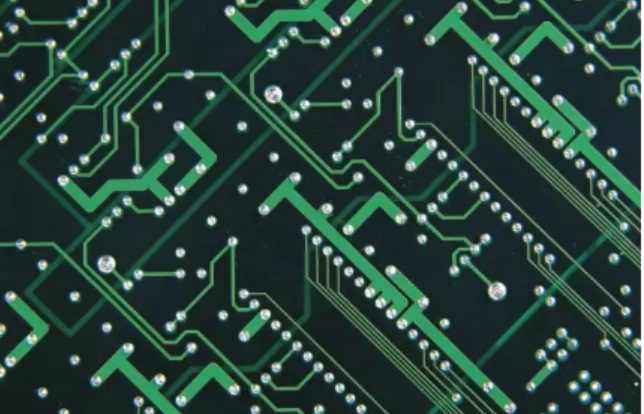
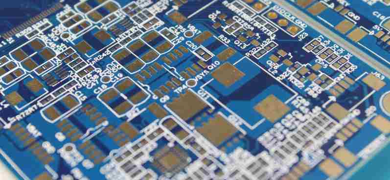
PCB (Printed Circuit Board), the Chinese name is printed circuit board, also known as printed circuit board, printed circuit board, is an important electronic component, is the support body of electronic components, is the electrical connection provider of electronic components. Because it is produced by electronic printing, it is called "printed" circuit board. PCB manufacturing methods include addition method and subtraction method.
Addition method: A printed board PCB in which conductive material is selectively deposited on a substrate without copper foil to form conductive patterns. There are screen printing electroplating method, paste method, etc.
Reduction method: On the coated copper plate, through the photochemical method, screen printing graphic transfer or electroplating graphic resist layer, and then etch off the non-graphic part of the copper foil or use mechanical way to remove the unnecessary part of the printed circuit board PCB. There are two main methods: engraving and etching. Engraving method is to remove the unnecessary copper foil by machining method, in a single piece of trial production or amateur conditions can be quickly produced printed circuit board PCB; Etching method is the use of chemical etching method to subtract the unwanted copper foil, which is currently the most dominant PCB manufacturing method. Now let's focus on etching.

1. pattern plating etch process
(1) The process takes the double panel as an example, the process is: blanking → drilling →PTH (electroless copper plating) → copper plating → photoimaging → graphic plating → alkaline etching → welding resistance + character → hot air smoothing (HAL) → Machining → Electrical performance test (ETest) →FQA→ finished product.
(2) Key points only conductive graphics for selective plating. Plate drilling, electroless copper plating, light imaging to form conductive graphics, this time only for the line and hole and pad graphic plating copper, so that the average copper thickness in the hole is greater than or equal to 20μm, and then tin plating (tin coating as etching resistance layer), remove the dry film (or wet film), alkaline etching, so as to get the required wire graphics. Return the tin coating on the surface and inside the hole, screen solder and character, hot air leveling, machining, electrical performance testing, to obtain the desired PCB.
(3) Features many processes, complex, but relatively reliable, can do fine line. Most European, American and Chinese enterprises use this process.
panel plaTIng etch process
(1) Process blanking → drilling →PTH (electroless copper plating) → plate plating → photoimaging → acid etching → welding resistance + character → hot air leveling (HAL) → shape machining → electrical test (E-Test) →FQA→ finished product.
(2) Key points
① After the plate is drilled and electroless copper plated (PTH), the whole plate and the hole are electroplated to the required copper thickness, so that the average copper thickness in the hole is greater than or equal to 20μm.
(2) Only the holes and figures were covered with dry film, and the dry film was used as the corrosion resistance layer.
③ The excess copper is etched in the acid etching solution to obtain the required wire pattern.
(3) Characteristics
The process is more simple than the graphic electroplating etching method, but the process control will be more difficult. Many Japanese enterprises use this process, and a small number of domestic enterprises use this method for mass production.
② Difficulty: It is difficult to control the uniformity of the thickness of the copper plating layer on the plate. The copper layer around the plate is thick and the middle is thin. It is difficult to etch evenly and the fine line is difficult to produce.
(4) Dry film cover hole, especially the hole with large aperture, such as not covered up, etching liquid into the hole, the hole copper is eroded, the plate can only be scrapped.
3 SMOBC method (solder mask over bare circuit)
Cover the bare copper wire with a flux shield and then hot air leveling. Either sink Ni/Au, Ag, Sn, or OSP (orgamic solderability preserrating). The purpose is to have no solder (Pb-Sn, or metal layer N i/ Au, Ag, Sn, OSP) on the wire, and only to coat the holes and pads with lead tin (or N i/ Au, Ag, Sn, OSP).
The function of this process is to prevent the printed board from causing line bridging during assembly welding; Save metal cost; Solder on the line to obtain good adhesion. If lead - tin solder is on the line, the choke layer of the line will be brittle when welding.
smobc is actually graphic electroplating etching. This method has been used for twenty or thirty years. In the 1970s and 1980s, after coating resist-welding on bare copper wire, hot air leveling was carried out, commonly known as tin spraying in Guangdong. The spray is lead-tin solder with a Pb: Sn of 37:63 or 40:60. This alloy has the lowest eutectic point of 183·C, and a Pb: Sn of 40:60 has a eutectic point of 190·C.
Hot air smoothing (tin-spraying) process, the Pb-Sn on the pad is not smooth enough, resulting in difficulties in mounting SMT on the surface. The pure gold has excellent solderability, and all the wires, holes and pads are plated with falx/gold (with brocade as the bottom layer). After etching, all except the holes and pads are coated with solder resistance, leaving only the holes and pads as N i/ Au. Instead of Pb-Sn, this is what people in Guangdong and Hong Kong call the water gold plate process. The gold layer is 24 karat pure gold, solderable, very thin, only.05 ~ 0.10μm. The base should be plated with nickel, 2~5μm thick, then plated with water gold. The gold content in the gold-plated groove is not much, about Ig/L gold. It should be noted that the weldability of thin gold is essentially different from the gold plating on the printed board plug. The gold plating of the plug is hard gold, wear-resistant, pluggable hundreds of times, requiring that the gold layer has a certain hardness, and the gold liquid in the gold groove contains trace cobalt (nickel, antimony) elements.
The use of lead in lead-tin alloys was banned by the European Union in July 2006 because of its toxicity. So SMOBC process surface coating into today's chemical leaching silver, tin, Ni/Au, OSP instead of Pb-Sn alloy. Wan Changbuqi, these processes in the final analysis belong to the graphic electroplating etching method SMOBC process.


Just upload Gerber files, BOM files and design files, and the KINGFORD team will provide a complete quotation within 24h.