
Professional PCB manufacturing and assembly
Building 6, Zone 3, Yuekang Road,Bao'an District, Shenzhen, China
+86-13410863085Mon.-Sat.08:00-20:00

With the rapid development of mobile phone, electronics, communication industry, but also promote the PCB circuit board industry continues to expand and rapid growth, people for the components of the layer, weight, precision, materials, color, reliability and other requirements are increasingly high.
However, due to the fierce price competition in the market, the cost of PCB board materials is also on the rise. In order to improve the core competitiveness, more and more manufacturers monopolize the market with low prices. However, behind these ultra-low prices, is to reduce the cost of materials and production costs to obtain, but the device is usually prone to cracks (cracks), easy scratches, (or bruises), its precision, performance and other comprehensive factors are not up to standard, seriously affecting the use of products on the weldability and reliability and so on.
In the face of various PCB circuit boards on the market, distinguish PCB circuit boards good or bad can start from two aspects; The first method is to judge from the appearance, on the other hand is to judge from the quality specification of PCB board itself.
The method of judging the quality of PCB circuit board
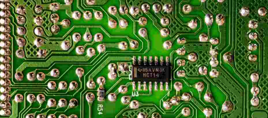
1, distinguish the quality of the circuit board from the appearance
In general, the appearance of PCB circuit boards can be analyzed and judged from three aspects:
Standard rules of size and thickness: The thickness of the circuit board to the standard circuit board is different sizes, customers can measure and check according to their own product thickness and specifications.

Light and color: the external circuit board is covered with ink, circuit board can play the role of insulation, if the color of the board is not bright, less ink, insulation board itself is not good.
Weld appearance: Because there are more parts of the circuit board, if the welding is not good, the parts are easy to fall off the circuit board, which seriously affects the welding quality of the circuit board. It is very important to have a good appearance, carefully identify and strong interface.
2. High-quality PCB circuit boards need to meet the following requirements
After the installation of the components, the telephone should be easy to use, that is, the electrical connection should meet the requirements
Line width, line thickness, line distance meet the requirements, so as to avoid line heating, open circuit, and short circuit.
High temperature copper skin is not easy to fall off.
The surface of copper is not easy to oxidize, which affects the installation speed.
No additional electromagnetic radiation.
The shape is not deformed, so as to avoid the deformation of the shell and dislocation of the screw hole after installation. Now the installation is mechanized, the hole position of the circuit board and the deformation error of the circuit and the design should be within the allowable range.
And high temperature, high humidity and special environment should also be considered.
The mechanical properties of the surface shall meet the installation requirements.
The above is the PCB circuit board judge good or bad method, in the purchase of PCB circuit boards, we must polish our eyes.
The technical realization process of PCB copying board is simply to scan the circuit board of the copying board, record the location of the components in detail, and then disassemble the components to make BOM and arrange material procurement. The empty board is scanned into pictures, processed by the copying software and restored to the pcb board drawing file, and then the PCB file is sent to the plate maker to make the board. After the board is made, the purchased components are welded to the PCB board, and then the circuit board is tested and debugged.
First, PCB copy board concrete steps
1. Get a PCB, first record the type, parameters and position of all the components on the paper, especially the direction of diode, three-stage tube and IC notch. It is best to take two pictures of the location of the key parts with a digital camera. Now the pcb circuit board more and more advanced above the diode triode some do not pay attention to see.
2. Remove all the multilayer plate copying parts, and remove the tin from the PAD hole. The PCB is cleaned with alcohol and placed in a scanner, which scans with slightly higher pixels to get a sharper image. Then the top and bottom layers are lightly polished with gauze paper until the copper film shines, put them in the scanner, start PHOTOSHOP, and sweep the two layers in color separately. Note that PCB must be placed horizontally and vertically in the scanner, otherwise the scanned image cannot be used.
3. Adjust the contrast and brightness of the canvas to make the contrast between the part with copper film and the part without copper film strong, then turn the sub drawing to black and white, check whether the lines are clear, if not, repeat this step. If it is clear, save the picture as black and white BMP format files TOP.BMP and BOT.BMP. If there is any problem with the picture, you can use PHOTOSHOP to repair and correct it.
4. Convert the two BMP files into protel files respectively, and import two layers into PROTEL. If the positions of PAD and VIA after two layers are basically identical, it indicates that the previous steps have been done well. So pcb copy board is a very need patience, because a little problem will affect the quality and copy board after the matching degree.
5. Convert the BMP of the TOP layer to the TOP.PCB, pay attention to the SILK layer, that is, the yellow layer, then you trace the line on the TOP layer, and place the device according to the drawing of step 2. Delete the SILK layer when you are done. Repeat until all layers are drawn.
6. Import TOP.PCB and BOT.PCB in PROTEL, and it is OK to combine them into a figure.
7. Use a laser printer to print the top layer and bottom layer respectively on the transparent film (1:1 ratio), put the film on the PCB, compare whether it is wrong, if it is right, you are done.
A copy of the original board was created, but it was only half done. But also to test, test copy board electronic technology performance is the same as the original board. If it's one, it's really done.
Remarks: If it is multi-layer board but also carefully polished to the inside of the inner layer, at the same time repeat the third to the fifth step of copying board steps, of course, the naming of the graphics are different, according to the number of layers, the general double panel copying board is much simpler than the multi-layer copying board, multi-layer copying board is prone to inaccurate situation, So the multilayer board copy board to be particularly careful and careful (which internal through holes and non-through holes are easy to appear problems).


Just upload Gerber files, BOM files and design files, and the KINGFORD team will provide a complete quotation within 24h.