
Professional PCB manufacturing and assembly
Building 6, Zone 3, Yuekang Road,Bao'an District, Shenzhen, China
+86-13410863085Mon.-Sat.08:00-20:00

In almost every metric used today, designers cite noise as one of the greater concerns and hazards to their designs. The adverse effects of noise on electronic circuits, including power supplies, have been well documented and are worth your while. So why does noise bother the whole design? What is causing concern is the unpredictability of the noise itself. Typically, the noise may come from an external source or an internal source. Even the source of the noise poses more problems.
In the case of an external noise source, it is technically an uncontrollable source. This means that designers will need to be diligent and creative in order to counteract these effects. For an internal source, although it may be easier to control, the results are still the same as for an external source. These include adverse effects on functionality, performance, accuracy and even consistency. In some cases, it can prevent the device from achieving the desired design goals anywhere from the prototype stage to production, or even failing to complete the failure.
The importance of reducing power supply noise
Although a lot of noise may be generated, the overall effect of this parameter is unfavorable. The consensus here is to address noise at the circuit level rather than at the power level. However, this solves only half the problem and most likely misses the more critical aspect of noise mitigation. The reason for this evaluation is because we build the circuits, and even the foundations of the system, based on the power supply's ability to function properly. Our company will study the manufacturing cost analysis in PCB design to reduce the production cost of PCB board. Suzhou MCU PCB design how much money
PCB design needs to consider the power consumption of resistance and calculate the power consumption of key resistors. Hefei simple PCB design wiring
PCB design latent circuit analysis
To ensure design reliability, latent circuit analysis provides a detailed path analysis for each identified path and applies component and path problems to all components in the path. This detailed analysis ensures that no latent paths exist. Another type of analysis is to ask questions about individual components when searching for latent indicators and latent labels. Digital latent analysis considers digital circuits and any design problems that can cause incorrect signal timing, switching, or mode errors.

When used in conjunction with circuit design, latent circuit analysis uses OrCAD to capture schematics and generate system netlists. In this way, latent circuit analysis can determine whether a bidirectional current path can be a latent path. The analysis is done by modeling all power switching components and all passive components. Instead of showing a model of an integrated circuit, the analysis shows how the IC has a switching circuit. This method relies on both functional positioning and design positioning. Hefei simple PCB design wiring
Shanghai Taofang Electronic Technology Co., Ltd. is committed to electrical and electrical, is a service-oriented company. The company's business is divided into circuit board development, embedded development, Internet of Things solutions, software development, and so on. At present, we continue to innovate and improve services to provide customers with good products and services. The company engaged in electrical and electrical for many years, with innovative design, powerful technology, and a group of professional team, to ensure that to provide customers with good products and services. Taofang Electronics is based on the national market, relying on strong research and development strength, integration of cutting-edge technology concepts, quickly respond to the changing needs of customers.
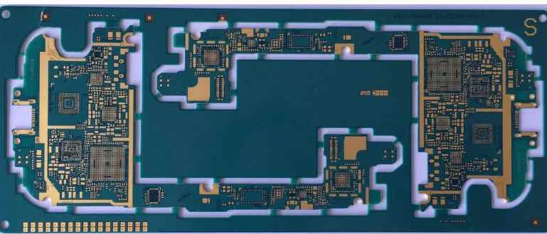
How to judge the quality of PCB design is as follows for your reference:
1. Standard rules for size and thickness. Customers can measure and check their own product thickness and specifications.
2. Light and color. External circuit boards are covered with ink, circuit boards can play the role of insulation, if the color of the board is not bright less ink, then PCB itself is not good.
3. Appearance of weld. There are many PCB parts. If the welding is not good, the parts will fall off easily, which will seriously affect the welding quality.
4. After the installation of components, the telephone should be easy to use, that is, the electrical connection should meet the requirements.
5, line width, line thickness, line distance meet the requirements, so as to avoid line heating, open circuit, and short circuit.
6, by high temperature copper is not easy to fall off. 7, copper surface is not easy to oxidize, affect the installation speed, oxidation after use soon after bad.
8. No additional electromagnetic radiation.
9. The shape is not deformed, so as to avoid the deformation of the shell and dislocation of the screw hole after installation. Now the installation is mechanized, the hole location of the circuit board and the deformation error of the circuit and the design should be within the allowable range.
10. High temperature, high humidity and special environment should also be considered.
11. The mechanical properties of the surface should meet the installation requirements. RF PCB design for high quality assembly and performance. Hefei double-sided PCB design
How to optimize PCB design for assembly process planning
Design a PCB layout, which is the direction or blueprint for building an electronic circuit board. For these designs, materials, dimensions, components and boreholes must be precisely specified for the contract manufacturer (CM) to construct the plates. Moreover, most engineers know that manufacturability improves if CM's manufacturing Design (DFM) rules are followed. It follows naturally that PCB designs for assembly process planning should lead to better results during the assembly phase of manufacturing.
PCB assembly or PCBA is the stage of circuit board manufacturing, which also includes the manufacturing process. Therefore, assembly provides the opportunity to inspect your board and make any corrections prior to shipping. However, the main function of this stage is to securely install the assembly, which is done by welding. The components used define the assembly process type, as shown below.
Through hole
The through-hole technique (THT) involves installing and connecting through-hole components using through-holes extending from the top to the bottom of the plate.
Surface mounting
Surface Mount technology (SMT) is an assembly process for fixing surface mount components, which may be connected to other plate elements using fan out or through holes.
There are many PCB design companies, how do you choose?


Just upload Gerber files, BOM files and design files, and the KINGFORD team will provide a complete quotation within 24h.