
Professional PCB manufacturing and assembly
Building 6, Zone 3, Yuekang Road,Bao'an District, Shenzhen, China
+86-13410863085Mon.-Sat.08:00-20:00

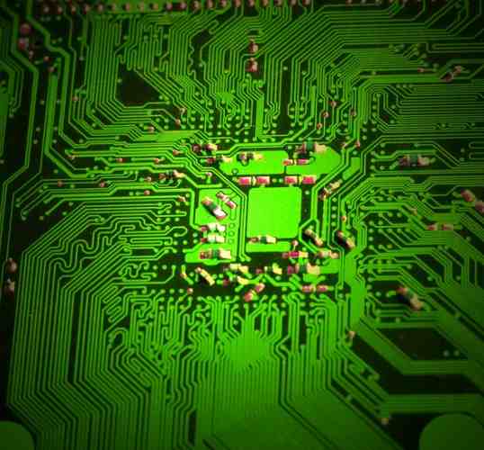
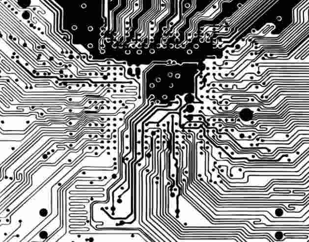
If this is the case, a PCB routestarts at one layer on the PCB board (reference to the signal return plane), passes through the hole and reaches another layer (which uses a different reference plane) as shown in the figure below. If the two reference planes (i.e. the path where the signal returns) have the same potential and the two layers are joined together multiple times through the holes, then the specified return path will have a small loop area. This is the design we wanted.
When the digital signal is referred to two different planes, one or more holes should be used between the two layers at the crossing point of the signal PCB routing if the potential of the two planes is the same. If the two planes have different potentials, two or more sutured capacitors should be used whenever possible to connect the two planes at the crossing point of the signal, preferably in a symmetrical manner.
However, if two reference planes have different potentials; For example, the signal return plane and the power plane, then the return path may be poorly planned and designed, thus forming a detour route with a large loop area, which will occur the often mentioned problem of the route across the division or crack.
In order to better plan the return path of the signal current, additional pass holes are placed where the signal PCB crosses the second reference plane at the beginning of the routing design.
If the circuit is complex enough that there may be too many changes in the reference plane, then a more laminated design may be needed to add additional signal or power return layers.
Note: For optimal high-frequency noise suppression, the power return "sandwich" layer spacing should be small - 3 to 4mil is generally considered ideal.

Generally, a spacing of 3 to 4mil between the power supply and the power return plane provides a good high-frequency bypass. Therefore, the decoupling capacitor should be evenly placed around the base surface. However, if a more traditional 10mil spacing is used, then the decoupling capacitors must be physically placed as close as possible to the VCC pins of each IC.
Another common mistake is to route a digital or high-power analog PCB through a sensitive analog part of the circuit. When wiring the digital PCB lines through the noiseless analog return plane, the digital switching noise usually interferes with the low level analog signal.
Note: When changing the reference plane twice, this forces the return current away from the path with the least impedance, which is the most common cause of common-mode current.
At the same time, the following five aspects should be paid attention to in the design:
one Ground and lap
In the field of EMI fault rectification, grounding actually refers to the analysis and design of the return path of circuits or components within a product. In practice, grounding often refers to the return path of a signal or power supply rather than the ground or ground plane.
To prevent misunderstanding, especially for EMI analysis, grounding also refers to the safety wire used to ground the product to the ground. Lap joint: refers to a low impedance connection between two conductive materials, usually metal sheets or shielded layers of a cable. Multiple lap or connected points should have low DC impedance between them. Such as less than 10 megohm, although many standards require less than 2.5 megohm or smaller. Good lapping ensures a solid path for current flow including high frequency current.
The key problem is that the current must flow unimpeded back to the noise or energy source. In practice, there is no such magic hole or spot in the ground where the noise current flows in large quantities or disappears. Therefore, in the analysis of EMI problems, using the signal or power return path or reference ground can more accurately express the correct EMI design concept.
two The clearance on the product housing
The gap in the metal housing of the product begins to act as an effective radiating antenna when the length is greater than approximately 1/10 of the wavelength corresponding to any of the many harmonic frequencies produced by the product. Since the antenna can transmit as well as receive, these gaps also allow external RF or pulse energy to enter the product, causing circuit disruption and misoperation of internal signals. In addition, any component, such as the LCD, must also be bonded in multiple points, as shown below.
The lapping of LCD components to the shielding housing is important for emission reduction
Note: When evaluating the integrity of the shield housing lap, metallic adhesive copper tape or aluminum foil are good diagnostic tools. Be sure to use these viscous copper strips for continuous conductivity.
Three. The lap of a cable
It is also very important that the conductive housing of any I/O or power connector is well bonded to the shielded housing of the product. Since a complete circle such as 3600 lap helps prevent radiation from the cable, it is best to use this lap only. As shown in the picture below.
The relationship between cable lapping and shielding and electromagnetic compatibility
Four. shield
Metal shields can be used as high frequency field barriers. Most products have a metal housing that completely encloses the circuit or a metal-coated plastic housing. For this reason, it is important to ensure that all the parts of the product shell are properly bonded together. When it is necessary to connect the cable through the product housing requires a certain skill. Unless the cable connector is lapped to the housing, common-mode noise current will leak along the connecting cable lead or the outer layer of the cable shield. The key here is the lap joint. This must be a very low impedance = 10mΩ or smaller connection. A 3600 lap should ideally be made to the product housing, as shown in the figure above. That is, all sides of the connector should be lapped with the product housing. This means that coatings such as paint, plating, etc. will prevent good bonding. Therefore, a low impedance 3600 lap will achieve the best results.
Five. filtering
Filters are often used in well-designed products. They are designed to block high-frequency currents - which can create the flow of radiative emission current or prevent pulsed energy such as ESD, power line transients, or radio-frequency current from entering the circuit. Products whose shell design is unshielded must rely on filtering and good PCB design to meet EMI requirements. For example, the following methods are commonly used:
(1) The input and output of the switching power supply need to be filtered to smooth the DC output and prevent the switching noise current from being transmitted through the input wire of the power supply.
(2) The reset pin of microcontroller IC is usually equipped with RC filter.
(3) I/O data lines and power lines use RC filters or common mode chokes.
(4) The ferrite clamped on the I/O cable can be used as a high-frequency choke.
Note: The purpose of the filter is to establish a high impedance to block the RF current flowing on the connecting wire cable or to provide a low impedance path for the current to return to the local energy source. It is usually best if these two goals can be achieved. For details of the filter design, please refer to Electromagnetic Compatibility Analysis and Design of iot Products.


Just upload Gerber files, BOM files and design files, and the KINGFORD team will provide a complete quotation within 24h.