
Professional PCB manufacturing and assembly
Building 6, Zone 3, Yuekang Road,Bao'an District, Shenzhen, China
+86-13410863085Mon.-Sat.08:00-20:00


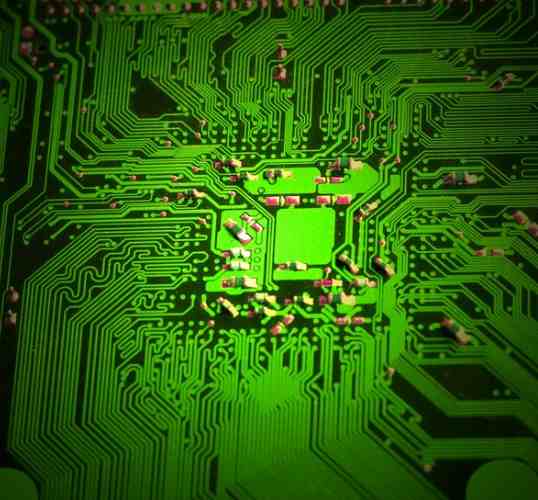
High-tech development, people need high performance, small size, many functions of electronic products, to promote printed circuit board manufacturing also to light, thin, short, small development, limited space, to achieve more functions, wiring density increases, aperture * small. From 1995 to 2007, the volume capacity of mechanical drilling for small holes decreased from 0.4mm to 0.2mm or even smaller. The size of the metallization hole is also getting smaller. Layer to layer interconnect depends on the metallized hole, quality directly related to the PCB performance. With the reduction of the aperture, the original debris that has no effect on the larger aperture, pcb board factory, such as brush debris, volcanic ash, once remaining in the hole, will make the chemical precipitation of copper, copper plating will lose effect, there is no copper hole, become the reason for the metalization of the hole

Common circuit board and multilayer PCB circuit board difference pcb
If you can see the naked eye multi-layer PCB circuit board and usually PCB circuit board people, then I will not say, PCB multi-layer circuit board and PCB double-sided circuit board appearance if you do not pay attention to the difference is not visible, because the appearance is basically the same, maybe someone will ask! Isn't a multilayer circuit board a lot of layers? How to see is also a board ah? The offer is still so much higher.
The number of layers of the original multilayer circuit board is the inner layer, 1-2 layers check 1 layer PCB single panel, 2 layers referred to as PCB double panel, 3-48 layers more called PCB multilayer board, the higher the number of layers, the higher the unit price, because the inner layer of the line is to press, press this process is not high technical content, the machine cost is relatively high, If you want to rent equipment, that is, a day is 1000-5000 this offer, buyout that less is also 2 million - 10 million! In the buy is not cost-effective, after all, it is high-tech, follow-up repair has certain difficulty, technical content is equal to the cost, we all know that the quality of the multilayer circuit board is very strict. Scrap a little bit in the previous process, then all the pcs specification pins are scrapped. If after the process scrap, there is a little bit of abnormal quality, the previous process is equal to dry for nothing.
So how do we distinguish a piece of product is usually PCB double panel or multilayer PCB circuit board?
1. The more the number of layers, the larger the shadow in the sheet material;
2.PCB double panel is the line and ink at both ends;
3.PCB double-sided pcb board can not see the line inside the board, is pure board, pcb, pure glass fiber;
4. If the board is die punching, you can use your hand to insert the edge of the board, *pcb board, so that the board is smooth and recognizable;
5. Multilayer PCB board board can see the faint shadow, a little dim, deep can see the line;
6. The multilayer PCB board material is usually the use of KB material, contrast smooth, especially in the molding processing after cleaning can be seen;
7. In the end how to distinguish several layers of several layers of boards, accurate data can only be recorded by the manufacturer's IM inspection or the development engineer's drawing board.
Vacuum laminating machine, reduce the pressure to reduce the flow of glue, as far as possible to maintain more resin, because the resin affects the εr, resin preservation more, εr will be lower. Control lamination thickness tolerance. Because the PCB board thickness is not uniform, it indicates that the change in the thickness of the medium will affect Z0.
Strictly according to customer requirements of PCB circuit board type blanking, type wrong, εr wrong, wrong board thickness, PCB manufacturing process is all right, the same scrap. Because Z0 is greatly affected by εr, the finished multilayer board should avoid water absorption as far as possible, because the εr = 75 of water, will bring great drop and instability effect on Z0.
The solder resistance of PCB board surface will reduce the Z0 value of the signal line by 1 ~ 3Ω. Theoretically, the solder resistance thickness of pcb board should not be too thick. In fact, the influence is not very great. The surface of the copper wire is in contact with air (εr = 1), so the Z0 value is high. However, Z0 value will decrease by 1 ~ 3Ω after welding resistance, because the εr of welding resistance is 4.0, which is much higher than the air.
The inner plate must find the wire gap, convex, for 2GHZ high-speed signal, even 0.05mm gap, also scrapped; Controlling inner line width and defects is key.
pcb- pcb board is provided by Shenzhen Youlutong Technology Co., LTD. Shenzhen Youlutong Technology Co., LTD. () adhere to the "people-oriented" business philosophy, has a dedicated staff, and strive to provide good products and services to the society, and welcome new and old customers to visit, sincere cooperation, create a better future.


Just upload Gerber files, BOM files and design files, and the KINGFORD team will provide a complete quotation within 24h.