
Professional PCB manufacturing and assembly
Building 6, Zone 3, Yuekang Road,Bao'an District, Shenzhen, China
+86-13410863085Mon.-Sat.08:00-20:00

FPC flexible circuit board production process and process requirements
PCB manufacturers, PCB designers and PCBA manufacturers explain FPC flexible circuit board production process and process requirements
Printed circuit boards, also known as printed circuit boards, are providers of electrical connections for electronic components.
Printed circuit board is usually represented by "PCB", not "PCB".
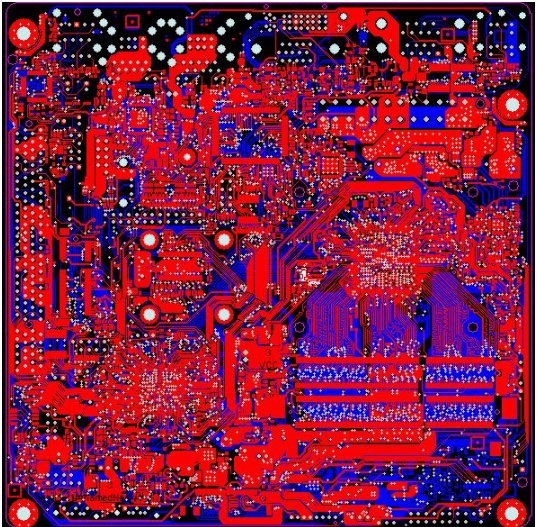
PCB design is mainly layout design; The main advantage of using circuit board is to greatly reduce wiring and assembly errors, and improve the automation level and production labor rate.
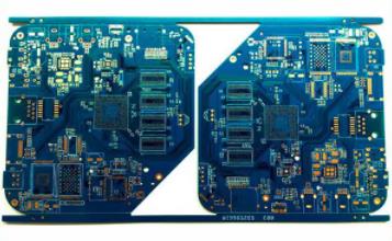
Printed circuit board can be divided into single panel, double panel, four layer board, six layer board and other multi-layer circuit boards according to the number of circuit board layers.
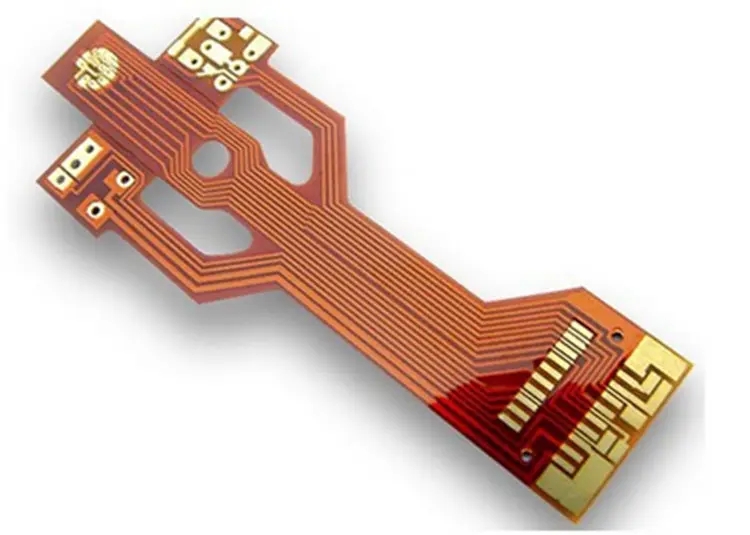
PCB circuit board was originally made of cardboard (old style radio). Now it is generally made of FR4 hard board and some special boards. Today's Flexible Printed Circuit (FPC) is a highly reliable and excellent flexible printed circuit board made of polyimide or polyester film. It has the characteristics of high wiring density, light weight, thin thickness and good bending performance. It is mainly used in light and thin electronic products such as mobile phones, laptops or LCD screens.
The core layer of this kind of circuit board is ultra-thin polymer film. First, the polymer film will be sandwiched between two copper sheets by the machine.
After being uniformly cut into rectangular sheets on the machine, separate them with laminates and put them in a pile.
Then it is sent to the vacuum pump box to close the layers together, and then sent to the high temperature and high pressure box for treatment for several hours. Since the polymer film in the middle layer has its own coating of heat activated adhesive, the original three layers will be bonded as a whole.
Next, the stack of pressing plates will be cut into fixed size plates and drilled with small holes for easy assembly, and then the fourth layer of photosensitive film will be stuck on the surface of the circuit board through the film applicator.
The technician draws the integrated circuit diagram with a computer according to the customer's needs, and then puts the board into the exposure machine. The computer will control the machine to conduct laser scanning of the photosensitive layer. The surface of the irradiated photosensitive layer will react and harden, so as to protect the copper layer below from pickling.
After cleaning the area not irradiated by the laser with the pickling machine, the copper layer left on the entire polymer film is the original computer drawn integrated circuit. Then, remove the dust on the surface with a sticky roller, and then place the fifth insulating layer.
Finally, the whole circuit board is separated by plastic paper and laminate and placed in a pile, and then sent to the vacuum pump box again to close the layers together, and then sent to the high temperature and high pressure box for several hours.
When the circuit board is cooled, it can be put into the mold manually. After the designated shape is made with a punch, a flexible circuit board is formally completed. PCB manufacturers, PCB designers and PCBA manufacturers will explain the production process and process requirements of FPC flexible circuit boards.


Just upload Gerber files, BOM files and design files, and the KINGFORD team will provide a complete quotation within 24h.