
Professional PCB manufacturing and assembly
Building 6, Zone 3, Yuekang Road,Bao'an District, Shenzhen, China
+86-13410863085Mon.-Sat.08:00-20:00

First of all, what should pcb proofing factories pay attention to? As a pcb proofing factory, first of all, after the customer places an order, we need to review whether the uploaded files meet the pcb process requirements of the factory, the manufacturing process capability, and whether the uploaded files have design problems. If the uploaded parameter information is inconsistent with the file, we must confirm with the customer at the first time which one shall prevail for production? Is the wiring diagram complete? If it is incomplete, it also needs to be confirmed with the customer; If the bottom screen print is the opposite of the top screen print, ask the customer whether they need to take the bottom as the positive or the positive as the bottom; The most important thing is that the pcb proofing factory must ensure the quality, delivery time and logistics, which is also the most concerned problem of customers.
Pcb proofing
There are mainly three kinds of pcb proofing factories. The common ones are professional sample factories, individual copying companies, and the best one is the formal pcb factory. Generally speaking, the formal pcb factories are long-term customers. After the completion of proofing, there will also be professional flying needle testing. Such factories must be the most guaranteed for customers. The professional pcb proofing factories generally only make one or two small boards, with small cost and small production, After completion, there will be no formal flying needle test. In this case, if the customer has problems after receiving the sample, such factory will not make relevant compensation. Therefore, we still need to choose a formal pcb proofing factory with delivery commitment and quality assurance to do the proofing.
What the pcb design engineer needs to pay more attention to is the parameter information, quantity and component packaging in the design process. During the design process, it is necessary to plan the whole circuit as a whole, whether there is a short circuit in the circuit, and whether the electrical inspection is in place. After all inspections are completed, the design engineer should first ensure that there is no packaging in the established packaging library, and then design the pcb board diagram, The components required in the drawing must be packaged in the packaging library to facilitate the smooth design; For the design parameters of pcb board, the designer needs to design the corresponding layers, colors, sizes, processes, etc. according to the requirements of the product circuit system; The designed pcb template drawing needs to generate a network table; The overall layout of pcb design drawing can adopt the combination method of automatic layout and manual layout, load the component packaging model into the appropriate position in the pcb design window, so that the component layout is more reasonable and beautiful. The wiring of pcb design drawing also needs attention. if the automatic wiring is not successful, manual wiring can be carried out; After all the designs are completed, save the designed pcb layout and then output the design documents. At last, there is an important step, which is board simulation analysis. In short, it is the signal simulation of pcb template, so as to analyze whether the layout and parameters of the whole circuit are reasonable. The ultimate goal is to consider the cost of pcb reasonable planning and product stability.
Documents to be provided during pcb proofing
It is the early stage of mass consumption. As long as the pcb proofing is accurate, it can be put into production in large quantities. Therefore, it is particularly important to provide accurate pcb proofing files. Do you know which pcb proofing files need to be provided? And what problems should we pay attention to in the documents provided?
Pcb proofing
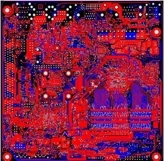
First of all, pcb proofing needs to provide pcb design or GERBER files, which should include plate making clarification - including detailed requests for board layers, materials, pad process, ink color, etc. Next, we will have a detailed understanding of the local main parameter clarification.
Data: To clarify what kind of pcb manufacturing data is required, FR4 is the most common one at present, and the main data is epoxy resin peeling fiber cloth board.
Plate layer: pcb proofing shall specify the number of layers for pcb plate manufacturing. (The manufacturing layers of pcb boards are different, and the prices are also different. The proofing process of pcb circuit boards is much the same.)
Soldering resistance color: There are many colors, which can also be stopped according to the request, and the common color is green.
Color of pcb silk screen printing: the color of the font and border of pcb silk screen printing, usually white.
Copper thickness: Generally, the copper thickness is calculated scientifically according to the current of the pcb circuit. The thicker the copper is, the better, but the cost will be higher, so the demand is reasonable and balanced.
Whether the vias can cover the resistance welding: the resistance welding is to insulate the vias, otherwise it is to make the vias uninsulated.
Exterior coating: tin spraying and gold plating.
Quantity: the quantity of pcbs manufactured in must be clearly stated.


Just upload Gerber files, BOM files and design files, and the KINGFORD team will provide a complete quotation within 24h.