
Professional PCB manufacturing and assembly
Building 6, Zone 3, Yuekang Road,Bao'an District, Shenzhen, China
+86-13410863085Mon.-Sat.08:00-20:00

How to clean and maintain PCB and how to deal with PCB pad loss
PCB manufacturers, PCB designers and PCBA manufacturers explain how to clean and maintain PCB, and how to deal with PCB pad loss
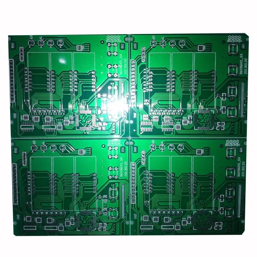
Recently, I have been assembling many USB PCB boards, which makes me think of the best way to clean them after assembly. "Dirty" flux is used in the assembly work, so theoretically I don't need to clean it, but if I don't do this, it will leave an ugly sticky mess. Unfortunately, the black solder mask of the retro USB board seems to highlight the flux residue more than other colors. I also recently started to use gel instead of flux pen in the syringe, which is thicker and leaves more residue. So good cleaning is more important than ever.
In the past, my standard cleaning method was to use an ordinary cotton swab with 99% isopropyl alcohol. It can dissolve flux residues, but this cotton swab can easily trip over the sharp corners of the parts, quickly become fragments, and leave small cotton fibers everywhere. Sponge cotton swabs and cloth head cotton swabs are used in the back. These cotton swabs are basically designed for industrial use. In any case, the packaging and winding of cotton are more tight than those of ordinary cotton swabs, and they are "low down", while showing superior wear resistance and cleaning performance, which can be repeatedly wiped. It helps to reduce cut and stray cotton fibers, but it cannot completely eliminate them,
As you can see here, isopropyl alcohol also leaves a residue that looks unattractive. Its visibility depends on the angle of light to a large extent, and I deliberately chose the photo with the worst angle. I'm not sure whether this residue is really from alcohol or whether it is dissolved in alcohol, but whether there are stripes on PCB when it is dry. I found that I needed to wait until it was dry, and then use another dry cotton swab to wipe the dry area and remove the stripes. The final result is still not perfect, although it is very good. However, the entire cleaning process can be very time-consuming, taking several minutes for each circuit board.
What to do if the pad of the circuit board is soldered off
When the circuit board is welded, the pad falls off because the welding time is too long or the temperature is too high due to repeated welding. The copper strip of the circuit board pad will fall off only after repeated expansion. Pay more attention to this during welding to prevent more falling off.
Cut off the detached bonding pad of the circuit board with a knife to the place where it does not fall off, so as to prevent the circuit from expanding along the falling place. If your component pin is long enough, you can scrape off the insulating paint at the circuit connector after cutting off, and solder the farsighted pin here If the component pin of your PCB circuit board is not long enough, you can use a piece of thin wire with good soldering tin to pass through the pad hole and then weld it to the component pin, and the other end is welded to the pad joint and fixed with hot melt adhesive to prevent the solder from falling off again
If the bonding pad of your circuit board falls off seriously, the above method is not suitable. You can also choose the flying wire method. One end of the wire is welded to the soldered component pin, and the other end is welded to any solder joint connected to the soldered pad Another way is bridging. If there are components on the same line around the soldered pad component pins, you can directly weld the component pins to the pins of that component and discard the original pad. Of course, you must see clearly that the string position cannot be soldered to prevent burning components.
PCB manufacturers, PCB designers and PCBA manufacturers explain how to clean and maintain PCB and how to deal with PCB pad loss.


Just upload Gerber files, BOM files and design files, and the KINGFORD team will provide a complete quotation within 24h.