
Professional PCB manufacturing and assembly
Building 6, Zone 3, Yuekang Road,Bao'an District, Shenzhen, China
+86-13410863085Mon.-Sat.08:00-20:00

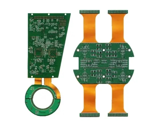
The reason why multilayer PCB boards are even layers
In the design scheme and production process of multilayer circuit boards, each layer must be symmetrical, and different sizes may cause distortion. In the production process, the four layer board is easier to control than the three layer board. The warpage of the four ply board can be controlled at 0.7%. It is lower than the IPC600 standard, but when the size of the three-layer board is large, the warpage will exceed this standard, and the warpage beyond this standard will affect the subsequent chip production and product quality.
In general, the design of double-layer PCB does not design odd layers. The difference between production and manufacturing is the cost of four layers of copper foil and adhesive layer. The cost difference is small. When the PCB manufacturer brings 3-4 layers as the level price, the price is defined by an even number. For example, if you design 5 layers of boards, the other party will quote the price of 6 layers of boards. That is to say, the price of the third floor of your design is the same as that of the fourth floor of your design. So why not choose the four ply board?
The double-layer PCB is mainly composed of the following layers: signal layer, internal plane, mechanical layer, mask layer, silk screen layer, and system layer. The signal layer is divided into top layer, middle layer and bottom layer, mainly used for assembling various components, or for wiring and welding.
Differences between PCB gold deposition and gold plating
What is PCB gold plate
The so-called PCB gold deposition processing process refers to the process of creating a layer of coating based on chemical oxidation and reduction, which is usually thin and thick. It is a type of chemical nickel gold gold deposition method, which can achieve a thicker gold layer.
What is PCB gold plate
PCB gold plating is also known as "electrogilding", "electrogilding", "electrogilding", "electrogilding", and "electrogilding". Electrogilding can be divided into soft gold and hard gold. Hard gold is used to gold finger pcb circuit board products. The basic principle is that nickel and gold (also known as gold salt) are melted into chemical solution, and the PCB circuit board is immersed in the electroplating process cylinder and connected with the working current to create a nickel gold coating on the copper foil surface of pcb circuit board. Because of the high hardness of the coating, The more wear resistant.
What is the difference between PCB gilding and electrogilding
1. The thickness of gold is thicker than that of electroplated gold, and the surface of the gold plated plate is golden yellow, which is more yellow than that of electroplated gold. From the surface, the gold plated plate can satisfy customers more.
2. The crystal structure caused by gold deposition is different from that caused by electroplating gold. Compared with electroplating gold, the gold deposition is easier to weld and is less prone to poor welding during welding. In addition, the gold deposition is softer than electroplating gold. The gold finger circuit weight plate is usually made by electroplating gold, and the hard gold has stronger wear resistance.
3. Compared with electroplated gold, the precipitated gold has a denser crystal structure and is not easy to be oxidized.
4. With the high-precision product wiring becoming more and more high-precision, some wire spacing and spacing have been as low as 3mil, which is easy to cause gold wire short circuit fault for high-precision plate electroplating process. However, only the welding layer of the gold plated plate has nickel gold, so there is no trouble of gold wire short circuit. Moreover, the resistance welding on the line is more firmly combined with the copper layer, and the engineering project will have any negative impact on the spacing when making data compensation.
5. For high-frequency boards with high relative demand, the flatness of the gold plate is also better, and the black mat problem will not occur after assembly. More importantly, the levelness and standby service life of the gold plated plate are also better than those of the gold plated plate.
Summarize 10 ways to select PCBA
Nov 14,2022


Just upload Gerber files, BOM files and design files, and the KINGFORD team will provide a complete quotation within 24h.