
Professional PCB manufacturing and assembly
Building 6, Zone 3, Yuekang Road,Bao'an District, Shenzhen, China
+86-13410863085Mon.-Sat.08:00-20:00

Have you learned the four steps of PCB inner layer processing!
Printed boards have developed from single-layer to double-sided, multi-layer and flexible, and still maintain their own development trends. Due to the continuous development towards high precision, high density and high reliability, and the continuous reduction of volume, cost and performance, the printed circuit board will still maintain strong vitality in the future development project of electronic equipment. 3、 Marks of printed board technical level:
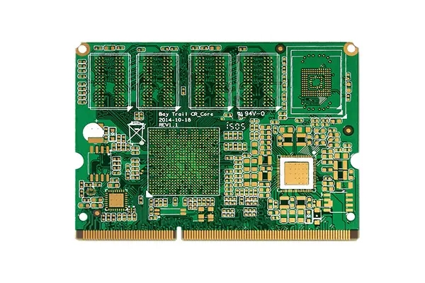
For double-sided and multilayer hole metallized printed boards, the mark of technical level of printed boards is that the double-sided metallized printed boards produced in large quantities can be marked by the number of wires that can be laid between two pads at the intersection of 2.50 or 2.54mm standard grids.
(1) Pretreatment In the process of processing printed circuit boards, first cut the copper foil substrate to a size suitable for processing and production, and then conduct pretreatment. Generally speaking. Pretreatment has two functions: first, it is used to clean the substrate after cutting, so as to avoid the adverse effects of grease or dust on the subsequent lamination; The other is to roughen the surface of the substrate properly by brush grinding, micro etching and other methods, so as to facilitate the combination of the substrate and the dry film. Generally, the cleaning solution and micro etching solution used for pretreatment.
(2) Clean room During the transfer of circuit graphics, the processing of printed circuit boards requires a very high degree of cleanliness for the studio. Generally, at least film pressing and exposure should be carried out in a ten thousand level clean room. In order to ensure the high quality of circuit graphics transfer, it is also necessary to ensure the indoor working conditions during processing. The indoor temperature is controlled at (2111) ℃ and the relative humidity is 55% - 60%, so as to ensure the dimensional stability of the substrate and the negative film. Only when the whole production process is carried out at the same temperature and humidity, can we ensure that the substrate and negative film will not shrink or swell. Therefore, the production areas in the current processing plants are equipped with central air conditioners to control the temperature and humidity.
Before the substrate is exposed, a layer of dry film needs to be pasted on the tomb board during processing. This work is usually realized by a film press, which can automatically cut the film according to the size and thickness of the substrate. The dry film generally has a 3-layer structure. The laminator pastes the film on the substrate with appropriate temperature and pressure, and then it will automatically tear off the plastic film on the side combined with the plate.
Because the photosensitive dry film has a certain shelf life. Therefore, the substrate after the laminating operation should be exposed as soon as possible. During the processing, the exposure is carried out with an exposure machine. The interior of the exposure machine emits high intensity UV lines (ultraviolet rays). It is used to irradiate the substrate covering the negative film and the film. Through image transfer, the image on the negative will be reversed and transferred to the dry film after exposure. Thus, the corresponding exposure operation port is completed.
(3) The etching line comprises a developing section, an etching section and a stripping section. The etching section is the core of this production line, and its role is to corrode the bare copper that is not covered by the dry film.
(4) After the completion of automatic optical inspection, the substrate after the inner layer is added must be strictly inspected. Then the next processing step can be carried out, which can greatly reduce the risk. In this plus stage, the inspection of board identification is carried out through the AOI machine to test the appearance quality of bare boards. When working, the processing personnel first fix the board to be inspected on the machine table, and AOI uses a laser locator to precisely position the lens to scan the entire board surface. Then the obtained drawings are abstracted and compared with the defective drawings to determine whether there is a problem in PCB circuit manufacturing. At the same time, AOI can also indicate the type of problem and the specific location where the problem occurs on the substrate.
Have you learned the four steps of PCB inner layer processing from PCB manufacturing, PCB design and PCBA processing manufacturers!


Just upload Gerber files, BOM files and design files, and the KINGFORD team will provide a complete quotation within 24h.