
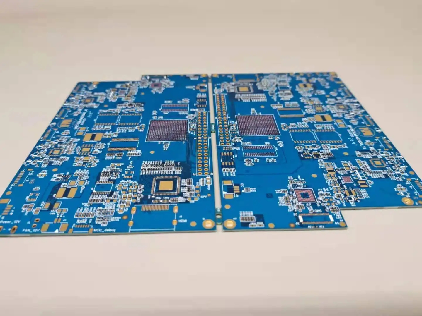
Professional PCB manufacturing and assembly
Building 6, Zone 3, Yuekang Road,Bao'an District, Shenzhen, China
+86-13410863085Mon.-Sat.08:00-20:00

Preliminary work, design considerations and PCB shelf life of PCB proofing
PCB manufacturers, PCB designers and PCBA manufacturers explain the preliminary work of PCB proofing, design considerations and PCB shelf life
1. The production of closed physical frames is a basic platform for future component layout and PCB proofing. Attention must be paid to accuracy. In addition, it is better to use circular arcs at corners, which can not only avoid being scratched by sharp corners, but also reduce the stress effect.
2. Introduce components and networks, and lay out components. When introducing components and networks into the drawn border during PCB proofing, you must carefully follow the prompts, including component packaging form and component network problems. It is not easy to have problems because of the comparison prompts. During PCB proofing, the layout of components and wiring have a great impact on the product life, stability and electromagnetic compatibility, which should be paid special attention to. Generally speaking, the following principles should be followed: placement order, pay attention to heat dissipation.
3. PCB design and wiring, adjustment and improvement When PCB design and wiring, you'd better pay attention to the requirements of processing parameters, or go to a reliable PCB proofing manufacturer, and the defective rate will be greatly reduced. After the PCB design and wiring is completed, what we need to do is to make some adjustments to the text, individual components, wiring and copper coating (this work should not be too early, otherwise it will affect the speed and bring trouble to the PCB design and wiring), also for the convenience of production, debugging and maintenance.
4. It is necessary to check the network sometimes because the network relationship of the PCB drawn is different from the schematic diagram due to misoperation or negligence. So after drawing, you should check it first, and then carry out the follow-up work.
What should be paid attention to in PCB design and fabrication
PCB is widely used in electronic products, experimental instruments, computers and other electronic equipment. It is a crucial basic assembly component in electronic equipment. Therefore, in the case of PCB production, only when all walks of life are considered clearly, can the application of electronic products not easily encounter problems. So, what should be paid attention to when designing PCB?
1. Manufacturing type
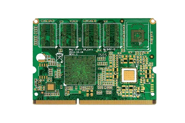
PCB circuit board is divided into single-sided aluminum substrate, double-sided circuit board and multi-layer circuit board. The conductivity pattern of single-sided aluminum substrate is relatively simple. Only the one side of the substrate has the conductivity pattern, while both sides of the double-sided PCB have the conductivity pattern. Typically, metal holes are used to connect double-sided conductivity images. With numerous layers and complex conductivity types, multilayer PCB circuit board is more suitable for high precision and complicated electronic products. Therefore, PCB manufacturers with guaranteed product quality need to consider which PCB must be used in the production process.
2. Raw materials of base materials
Polyimide film is composed of polymer materials, resin materials and modified raw materials, which can be used as the base material of CCL. There are many kinds of resin materials, such as urea formaldehyde resin, epoxy resin adhesive, PTFE, etc. There are two improved raw materials, namely paperboard and fabric surface, which depend on the physical properties of the substrate, such as cold resistance and tensile strength. Therefore, when making PCB, it is also necessary to consider which raw materials should be used for the substrate.
3. Non electrical performance index of copper clad laminate
The quality of CCL will directly damage the quality of PCB, and the quality of CCL is mainly shown in non electrical performance indicators such as peel strength, compressive strength, expansion and contraction, compressive strength, and immersion resistance. Therefore, the non electrical performance indicators of CCL should be taken into account when making PCB.
As PCB is the basic component of electronic products, it is necessary to use high-quality PCB. Therefore, customers should not only find PCB manufacturers with good after-sales maintenance services to produce PCBs, but also consider all aspects of PCB when making PCB and try to make the PCB design meet the application requirements.
Talking about the shelf life of PCB
As far as surface technology is concerned, gold melting and electrogilding have the longest storage time. Under the condition of constant temperature and humidity, the surface technology of tin spraying, electrogilding, gold melting and silver electroplating adopts vacuum packaging with a storage life of 6 months, while other surface technologies, such as silver precipitation, silver precipitation and OSP, can generally be stored for 3 months. Among them, the storage life of OSP (i.e. oxidation resistant plate) is the shortest after opening the package, It is better to use it as soon as possible, or the copper on the surface of the board will be oxidized. Generally, the PCB board should be placed in a dry and ventilated place, and the seasonal changes of sunlight and temperature and humidity should be avoided. These will affect the storage of the PCB board, especially the humidity has a great impact on the PCB function, and will attack the hole wall and surface metal. PCB manufacturers generally purchase vacuum packaging which affects the welding effect. If there is desiccant in the packaging, if the board is not used temporarily, it can not be unpacked for better preservation. If the oxidized boards need to be reused, they can be returned to the manufacturer for baking, reprocessing and other methods before use.


Just upload Gerber files, BOM files and design files, and the KINGFORD team will provide a complete quotation within 24h.