
Professional PCB manufacturing and assembly
Building 6, Zone 3, Yuekang Road,Bao'an District, Shenzhen, China
+86-13410863085Mon.-Sat.08:00-20:00

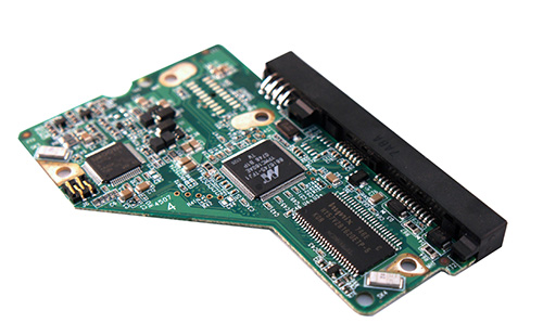
Common mistakes made by electronic manufacturers when explaining pcb processing
1. Common errors in schematic diagram:
(1) ERC reports that no signal is connected to the pin:
a. I/O attributes are defined for pins when creating encapsulation;
b. Inconsistent grid attributes are modified when creating or placing components, and pins are not connected to lines;
c. When creating a component, the pin direction is reversed, and it must be connected at the non pin name end.
(2) The component runs out of the drawing boundary: no component is created in the center of the component library chart paper;
(3) The created project file network table can only be partially transferred to pcb: global is not selected when generating netlist;
(4) Never use annotate when using components that are composed of multiple parts created by yourself.
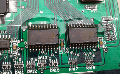
2. Common errors in PCB:
(1) When the network is loaded, it is reported that NODE is not found:
a. The components in the schematic diagram use packages that are not available in the pcb library;
b. Components in the schematic use packages with inconsistent names in the pcb library;
c. Components in the schematic diagram use packages with inconsistent pin numbers in the pcb library. For example, triode: pin numbers in sch are e, b, c, while those in pcb are 1,2,3.
(2) Always cannot print on one page when printing:
a. When creating the pcb library, it is not at the origin;
b. After moving and rotating the components for many times, there are hidden characters outside the boundary of the pcb board. Select to display all hidden characters, shrink the pcb, and then move the characters to the boundary.
(3) The DRC reporting network is divided into several parts:
This indicates that the network is not connected. Check the report file and select CONNECTED COPPER to find it.
In addition, remind friends to use WIN2000 as much as possible to reduce the chance of blue screen; Export the file several times to make a new DDB file to reduce the file size and the chance of the PROTEL being dead. If you make a more complex design, try not to use automatic routing.
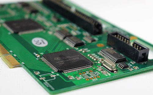
In PCB design, wiring is an important step to complete product design. It can be said that the previous preparations are all for it. In the whole PCB, the design process of wiring is the most limited, the most detailed, and the largest workload. PCB wiring includes single-sided wiring, double-sided wiring, and multi-layer wiring.
There are also two ways of wiring: automatic wiring and interactive wiring. Before automatic wiring, wires with strict requirements can be wired interactively in advance. The side lines of input and output terminals should avoid adjacent parallelism to avoid reflective interference. If necessary, ground wires should be added to isolate. The wiring of two adjacent layers should be perpendicular to each other, and parallelism is likely to cause parasitic coupling.
The routing rate of automatic routing depends on good layout, and the routing rules can be preset, including the number of bending times of routing, the number of through holes, the number of steps, etc. Generally, exploratory routing is carried out first, the short lines are quickly connected, and then maze routing is carried out. First, the lines to be routed are optimized globally. It can disconnect the already laid lines as needed, and try to re route to improve the overall effect.
I feel that the through-hole is not suitable for the current high-density PCB design. It wastes many valuable wiring channels. To solve this contradiction, blind hole and buried hole technologies have emerged. It not only completes the role of the through-hole, but also saves many wiring channels to make the wiring process more convenient, smooth, and perfect. The PCB design process is a complex and simple process. If you want to master it well, It also needs the majority of electronic engineering designers to experience themselves to get the true meaning.


Just upload Gerber files, BOM files and design files, and the KINGFORD team will provide a complete quotation within 24h.