
Professional PCB manufacturing and assembly
Building 6, Zone 3, Yuekang Road,Bao'an District, Shenzhen, China
+86-13410863085Mon.-Sat.08:00-20:00

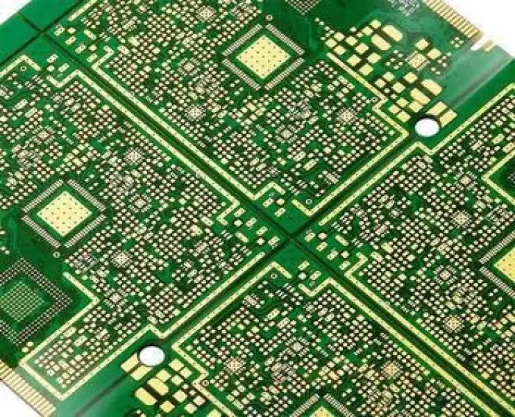
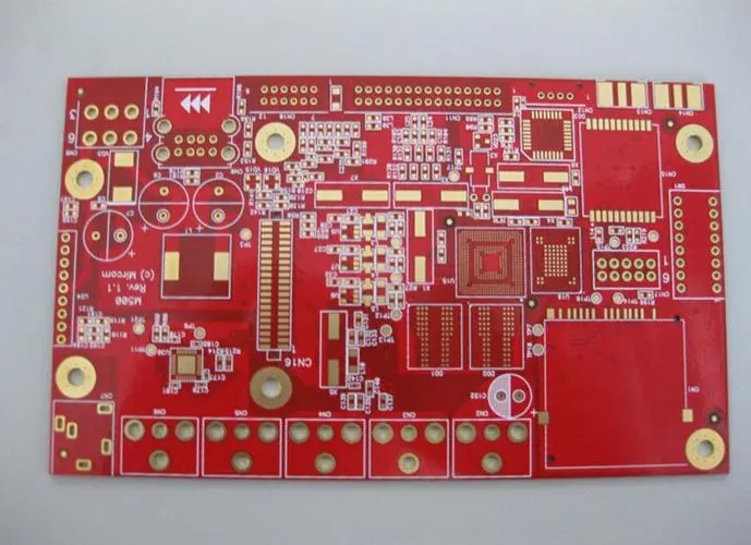
Prevent PCB board from bending and warping when passing through the reflow furnace
Prevent PCB board from bending and warping when passing through the reflow furnace
1. Effect of temperature reduction on plate stress
Since "temperature" is the main source of plate stress, the occurrence of plate bending and warping can be greatly reduced by reducing the temperature of the reflow furnace or slowing down the heating and cooling speed of the plate in the reflow furnace. However, there may be other side effects, such as solder short circuit.
2. Plate with high Tg
Tg is the glass transition temperature, that is, the temperature at which the material changes from glass state to rubber state. The lower the Tg value of the material, the faster the plate begins to soften after entering the reflow furnace, and the longer the time to become soft rubber state will be, of course, the more serious the deformation of the plate will be. The plate with higher Tg can increase its ability to withstand stress and deformation, but the price of materials is relatively high.
3. Increase the thickness of the circuit board
In order to achieve the goal of being thinner, many electronic products have left 1.0mm, 0.8mm and even 0.6mm thick plates. It is really difficult to keep the plates from deforming when they pass through the reflow furnace. It is recommended that if there is no requirement for being thinner, the plates should be 1.6mm thick, which can greatly reduce the risk of bending and deformation.
4. Reduce the size of circuit boards and the number of boards
Since most of the reflow furnaces use chains to drive the circuit board forward, the larger the size of the circuit board, the more it will sag and deform in the reflow furnace due to its own weight, so try to put the long side of the circuit board on the chain of the reflow furnace as the board edge, which can reduce the sag and deformation caused by the body weight of the circuit board. This is also the reason to reduce the number of boards, that is, when the furnace is said, The narrow edge shall be perpendicular to the furnace passing direction as far as possible to achieve the lowest concave deformation.
5. Use the furnace tray fixture
If the above methods are difficult to achieve, the last thing is to use the reflow carrier/template to reduce the deformation. The reason why the reflow carrier/template can reduce the bending warpage is that whether it is thermal expansion or cold contraction, it is hoped that the tray can hold the circuit board until the temperature of the circuit board is lower than the Tg value and the circuit board starts to harden again.
If the single-layer tray cannot reduce the deformation of the circuit board, you must add another layer of cover to clamp the circuit board with two layers of trays, which can greatly reduce the deformation of the circuit board through the reflow furnace. However, this tray is very expensive, and it needs to be manually placed and recycled.
6. Replace V-Cut with Router
Since V-Cut will damage the structural strength of the panels between circuit boards, it is better not to use V-Cut to divide boards or reduce the depth of V-Cut.
The circuit board manufacturer and circuit board design manufacturer explain how to prevent PCB from bending and warping when passing through the back soldering furnace.
Meaning and characteristics of common boreholes
Nov 04,2022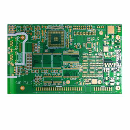


Just upload Gerber files, BOM files and design files, and the KINGFORD team will provide a complete quotation within 24h.