
Professional PCB manufacturing and assembly
Building 6, Zone 3, Yuekang Road,Bao'an District, Shenzhen, China
+86-13410863085Mon.-Sat.08:00-20:00

PCB common drilling in circuit board factory: through hole, blind hole and buried hole. The meaning and characteristics of these three kinds of holes.
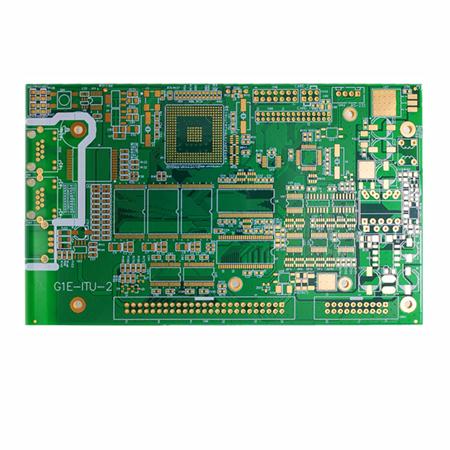
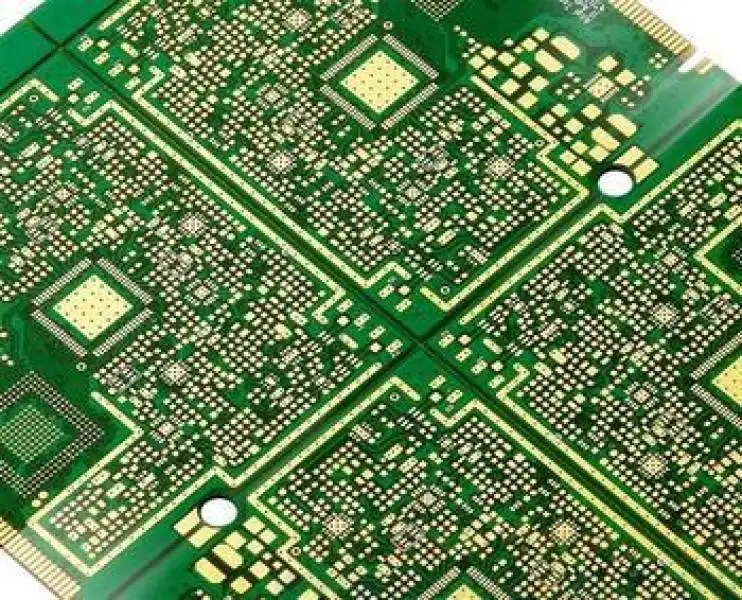
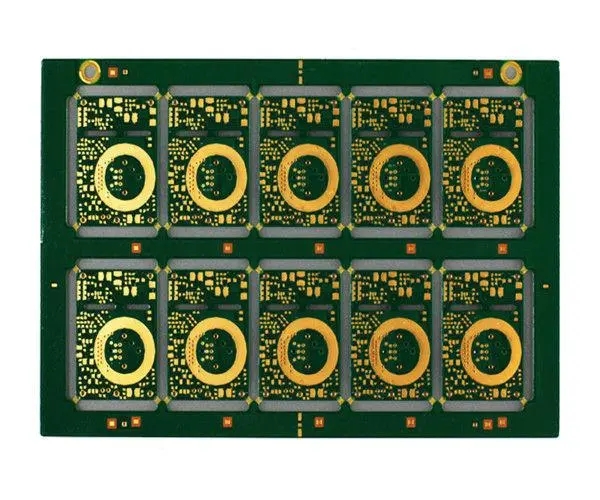
Circuit board factory

1 Through hole (VIA), a common hole, is used to conduct or connect copper foil lines between conductive patterns in different layers of the circuit board. Such as (such as blind hole and buried hole), but the copper plated hole of component guide leg or other reinforcement materials cannot be inserted.
Because PCB is formed by stacking and accumulating many copper foil layers, each layer of copper foil will be paved with an insulating layer, so that the copper foil layers cannot communicate with each other, and the signal link depends on the through hole (via), so it has the name of Chinese through hole. Features: In order to meet the needs of customers, the through hole of the circuit board must be plugged. In this way, in the process of changing the traditional aluminum plug hole process, the white screen is used to complete the resistance welding and plug hole of the circuit board surface, making it stable in production, reliable in quality, and more perfect in use. The through hole mainly plays the role of connecting and conducting circuits. With the rapid development of the electronic industry, higher requirements are put forward for the manufacturing process and surface mounting technology of printed circuit boards.
The process of conducting through hole to plug hole is applied, and the following requirements shall be met:
1. Copper can be found in the through hole, but plug can not be used for resistance welding.
2. There must be tin lead in the through hole, and there must be a certain thickness requirement (4um). There must be no solder blocking ink into the hole, which may cause tin beads in the hole.
3. The through hole must be provided with solder blocking ink plug hole, which is light tight, without tin ring, tin bead, flatness and other requirements.
2 Blind hole: It refers to connecting the outermost circuit in the PCB with the adjacent inner layer by electroplating holes. Because the opposite side cannot be seen, it is called blind through. At the same time, in order to increase the space utilization between PCB layers, blind holes are applied. That is, the through hole to one surface of the printed circuit board.
Features: The blind hole is located on the top and bottom surfaces of the circuit board, and has a certain depth. It is used to link the surface line and the inner line below. The depth of the hole usually does not exceed a certain ratio (aperture). This manufacturing method needs to pay special attention to the drilling depth (Z-axis) to be just right. If not, it will cause electroplating difficulties in the hole, so it is almost not used by the factory. It can also drill holes for the circuit layers that need to be connected in advance at the time of individual circuit layers, and then glue them together. However, it requires more precise positioning and alignment devices.
3 Buried hole refers to the connection between any circuit layers inside a PCB that is not connected to the outer layer, and also refers to the conductive hole that does not extend to the surface of the circuit board.
Features: In this process, it is impossible to use the method of drilling after bonding. Drilling must be carried out when individual circuit layers are used. First, the inner layer is partially bonded, then the inner layer is returned, and then the electroplating treatment is carried out. Finally, all the bonding can be carried out. It takes more time than the original through hole and blind hole, so the price is also the most expensive. This process is usually only used for high-density circuit boards to increase the usable space of other circuit layers
In PCB production process, drilling is very important and should not be careless. Because the drilling is to drill the required through-hole on the copper clad plate to provide the function of electrical connection and fixing components. If the operation is improper, there is a problem in the via process. The components cannot be fixed on the circuit board, which may affect the use, or even the whole board will be scrapped. Therefore, the drilling process is very important.


Just upload Gerber files, BOM files and design files, and the KINGFORD team will provide a complete quotation within 24h.