
Professional PCB manufacturing and assembly
Building 6, Zone 3, Yuekang Road,Bao'an District, Shenzhen, China
+86-13410863085Mon.-Sat.08:00-20:00

What preparations are made before SMT chip processing?
The circuit board manufacturer and the circuit board designer explain to you what preparations are made before the SMT chip processing and manufacturing process
SMT process and capability
SMT process: short for Surface Mount Technology, SMT surface mount technology is an electronic assembly technology that originated in the 1960s, was initially developed by IBM in the United States, and then gradually matured in the late 1980s. SMT technology is to install electronic components, such as resistors, capacitors, transistors, integrated circuits, etc. on printed circuit boards, and form electrical connections through lead soldering. The components used are also referred to as SMD (surface mount devices). The biggest difference between SMT and plug-in technology is that SMT surface adhesion technology does not need to reserve corresponding through holes for the pins of components, and the component size of surface adhesion technology is much smaller than that of plug-in packaging. This SMT technology can greatly reduce the volume of electronic products to achieve the purpose of thin and short, referred to as SMT process.
From the sample stage to the mass production stage, SMT needs to make detailed preparations before the SMT chip processing process to ensure that all materials can be successfully online and avoid various accidents of line stoppage and material finding. Since production efficiency is the lifeline of SMT chip processing, standardized production process management is particularly important. The following is a brief description of some preparations that must be done before SMT processing.
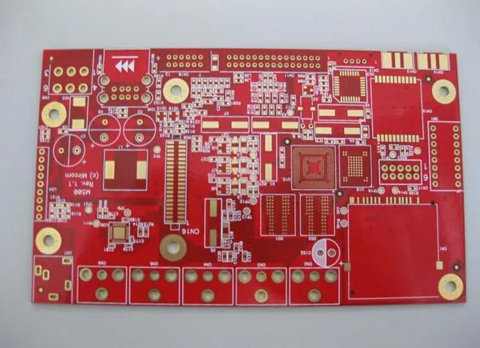
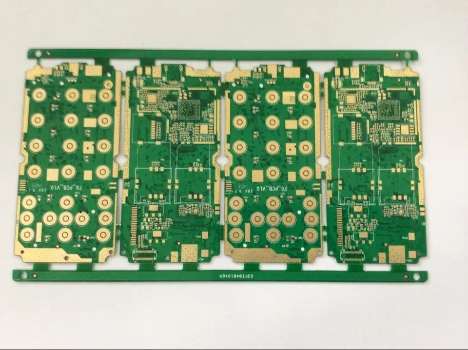
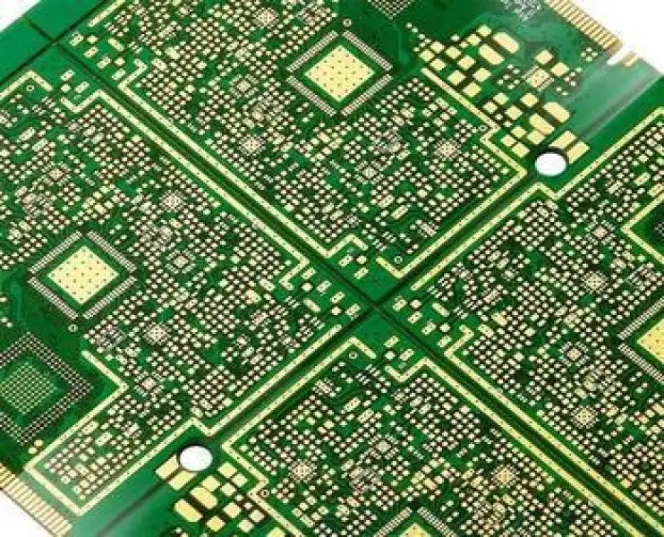
1. Circuit board information (Gerber)
● Electronic archives of standard circuit diagrams shall at least include 4 layers: PAD file, through hole file, text file and anti welding layer file.
● It is better to use the connecting Gerber provided by the PCB manufacturer.
● Standard plate edge specification: 10mm plate edge shall be reserved at the top and bottom respectively (as shown in the figure below).
● Specification of standard locating hole: one locating hole is located on the left and right of the same plate edge, and the center is 5mm from the plate edge on both sides, and 4mm from the plate edge.
● Specification of standard visual marking points: 1mm solid tin spraying dot with opposite diagonal asymmetry, 3mm diameter transparent ring of outer ring (as shown in the figure below).
Pcb locating hole
2. Bill of Materials (BOM)
● Position coordinates (CAD, text file with extension of ". TXT") shall be installed in electronic files.
● List of mixing SMT front and back materials with DIP materials (please provide the part coding principle and the resolution of front and back parts).
● Separate list of SMT front and back materials and DIP materials (please provide the resolution of front and back parts).
● Separate list of SMT front/SMT back/DIP materials.
3. Supporting information
● Furnace temperature measuring plate (including scrapped plate of important parts).
● Empty PCB.
● Printed steel plate.
4. Avoidance
● R/C and other parts for SMT shall not be made of granular bulk materials or cut ribbon bulk materials.
● IC and other main parts cannot be removed from PCB or used old products


Just upload Gerber files, BOM files and design files, and the KINGFORD team will provide a complete quotation within 24h.