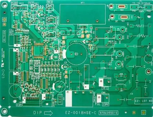
PCB problem: zebra strip also has problems
It was originally thought that [Zebra Strips] should be a simple part, but this incident was completely defeated by it. The reason is that one product of the company has designed an independent "Navigation key".
I don't know why the original design engineer chose to use the "Bama conductive adhesive strip" to connect the line between the main key and the navigation key, instead of designing the navigation key and the main key on the same key board, which may be due to some height difference (I guess, because it is already unavailable)!
This was not a big deal at first, but the problem occurred. The phenomenon was that after pressing some keys on the navigation key, it would move to other keys. If it was the same up, right, down and left buttons on the navigation key, it might be because of the poor design of the mechanism, which caused the misoperation of the adjacent key mechanism, but it was strange that the keys on the main keyboard actually moved, There is also a Bama conductive strip in the middle.
In order to identify whether this phenomenon is an electrical or mechanical problem, we directly remove the plastic and rubber buttons on the navigation buttons, expose the lines of the buttons directly, and then test the buttons with a conductive rod. As a result, the button linkage still occurs, so we can first eliminate the linkage problem caused by the button mechanism.

Next, there is only the problem of circuit board and zebra conductive adhesive strip. First, cross validation of zebra conductive adhesive strip was carried out. It was found that the button linked phenomenon followed the zebra conductive adhesive strip. In order to enable the production line to resume production immediately, a simple fixture was made from the existing product in an emergency. It is expected that this fixture can screen out the bad zebra conductive adhesive strip, but no defective product can be detected; Dismantle the zebra conductive tape and take it directly for insulation impedance and micro current test. It's embarrassing! In addition, no problems were found on the circuit board. Get stuck!
Cut the zebra conductive tape for inspection, and only one of the conductive tape was found to have a misplaced cutting deviation, which should be within a reasonable deviation range. How can we continue!
Later, I accidentally found that the gap between the gold finger on the circuit board and the zebra conductive adhesive strip seemed to be a little small. It seemed that there was no gap between at least two conductive strips as required, because the cutting of zebra conductive adhesive strip might have a deviation of one conductive strip (0.18mm). The mechanism assembly (upper and lower PCBA boards) and production error should also be 0.2mm, and the total tolerance should be at least 0.38mm, However, the actual measurement result of the minimum distance between golden fingers is only about 0.3mm, which is obviously insufficient! There should be a 0.5mm gap in the design of PCB Gerber when querying. Because there are vias, the golden finger is slightly biased, which is a damned error.
After reviewing the current design of the golden finger, the width of the contact pad is 0.8mm, the gap is 0.5mm, the pitch of the zebra conductive adhesive strip is 0.18mm, and the width of the contact pad should only be 0.64mm [=0.18mm x 3 (conductive strip)+0.1mm (tolerance)], which can ensure that at least three conductive strips are in contact with each contact pad. In addition to some allowable values, the width of the golden finger contact pad is changed to 0.7mm, and the gap is 0.6mm, which should completely solve this problem. In addition, do you want to consider moving the positions of the four vias slightly, or ask the PCB manufacturer to pay attention to the width and size of the contact pad of the golden finger, which should also solve this problem, but the key is how to prevent problems when looking for the 2nd source.
By the way, we can also consider changing the picth of Bama conductive tape from the current 0.18mm to 0.10mm.


