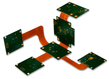
PCB professional service design and method
PCB professional service design and method
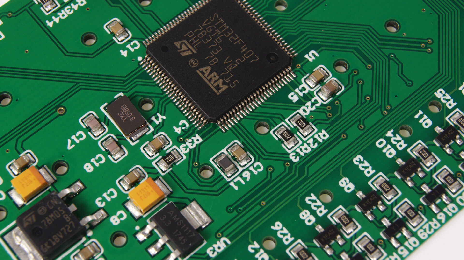
Whether you are a beginner in PCB design or a PCB design practitioner, "high-speed PCB design" is a design skill that everyone must master, including PCB design theory and design specifications and rules.
Rule analysis of some high-speed PCB designs
01
When designing the PCB layout, the design principle of laying in a straight line along the signal flow direction should be fully followed, and try to avoid going back and forth.
Cause analysis: Avoid direct signal coupling, which will affect the signal quality.
02
If the PCB clock frequency exceeds 5MHZ or the signal rise time is less than 5ns, multi-layer board design is generally required.
Reason analysis: This is the "55 principle" in PCB design. The signal loop area can be well controlled by using multi-layer board design.
03
In the multi-layer board, the TOP and BOTTOM layers of the single board should try not to have signal lines greater than 50MHZ.
Cause analysis: It is better to route the high-frequency signal between two plane layers to suppress its radiation to space.
04
On the PCB board, the filtering, protection and isolation devices of the interface circuit should be placed close to the interface.
Cause analysis: The effect of protection, filtering and isolation can be effectively realized.
05
If there are both filter and protection circuits at the interface, the principle of protection first and then filter should be followed.
Reason analysis: The protection circuit is used to suppress external overvoltage and overcurrent. If the protection circuit is placed after the filter circuit, the filter circuit will be damaged by overvoltage and overcurrent.
06
When laying out, ensure that the input and output lines of the filter circuit (filter), isolation and protection circuits are not coupled to each other.
Reason analysis: When the input and output lines of the above circuit are coupled with each other, the filtering, isolation or protection effect will be weakened.
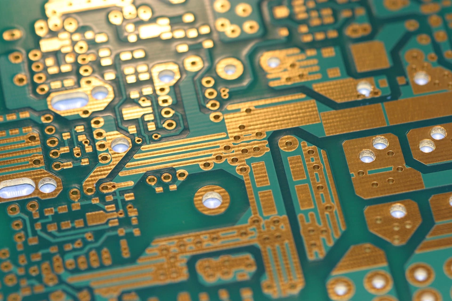
07
For multi-layer boards, key wiring layers (clock lines, bus lines, interface signal lines, radio frequency lines, reset signal lines, chip select signal lines, and various control signal lines) should be adjacent to the complete ground plane, preferably two ground planes. between planes.
Reason analysis: The key signal lines are generally strong radiation or extremely sensitive signal lines. Wiring close to the ground plane can reduce the area of the signal loop, reduce its radiation intensity or improve the anti-interference ability.
08
Key signal traces must not be routed across partitions (including reference plane gaps caused by vias and pads).
Cause analysis: Routing across partitions will lead to an increase in the area of the signal loop.
09
The key signal line is ≥3H from the edge of the reference plane (H is the height of the line from the reference plane).
Cause analysis: Suppress the edge radiation effect.
10
When there are high, medium and low speed circuits on the circuit board at the same time, the high and medium speed circuits should be kept away from the interface.
Cause analysis: Avoid high-frequency circuit noise radiating outward through the interface.
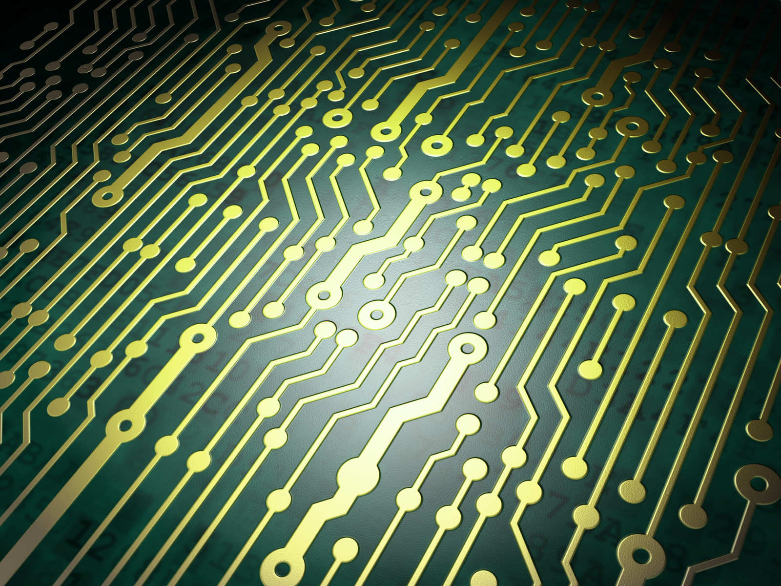
Knowledge expansion: what is "high-speed signal"
What is a high-speed signal? How to judge the high-speed signal? Cadence has defined this:
Any signal greater than 50MHz is a high-speed signal. Whether the signal is high-speed is not directly related to the frequency, but when the rising/falling edge of the signal is less than 50ps, it is considered a high-speed signal. When the length of the transmission path where the signal is located is greater than 1/6λ, the signal is considered to be a high-speed signal. When the signal is transmitted along the transmission path and suffers from severe skin effect and ionization loss, it is considered to be a high-speed signal. (The content of the graphic and text is organized by Quick PCB from the Internet)
With the increasing signal rates of today's electronic products, "high-speed signaling" has become very common in PCB design. Therefore, whether you are a beginner in PCB design or a PCB design practitioner, "high-speed PCB design" is a design skill that everyone must master, including PCB design theory and design specifications and rules.
Rule analysis of some high-speed PCB designs
01
When designing the PCB layout, the design principle of laying in a straight line along the signal flow direction should be fully followed, and try to avoid going back and forth.
Cause analysis: Avoid direct signal coupling, which will affect the signal quality.
02
If the PCB clock frequency exceeds 5MHZ or the signal rise time is less than 5ns, multi-layer board design is generally required.
Reason analysis: This is the "55 principle" in PCB design. The signal loop area can be well controlled by using multi-layer board design.
03
In the multi-layer board, the TOP and BOTTOM layers of the single board should try not to have signal lines greater than 50MHZ.
Cause analysis: It is better to route the high-frequency signal between two plane layers to suppress its radiation to space.
04
On the PCB board, the filtering, protection and isolation devices of the interface circuit should be placed close to the interface.
Cause analysis: The effect of protection, filtering and isolation can be effectively realized.
05
If there are both filter and protection circuits at the interface, the principle of protection first and then filter should be followed.
Reason analysis: The protection circuit is used to suppress external overvoltage and overcurrent. If the protection circuit is placed after the filter circuit, the filter circuit will be damaged by overvoltage and overcurrent.
06
When laying out, ensure that the input and output lines of the filter circuit (filter), isolation and protection circuits are not coupled to each other.
Reason analysis: When the input and output lines of the above circuit are coupled with each other, the filtering, isolation or protection effect will be weakened.
07
For multi-layer boards, key wiring layers (clock lines, bus lines, interface signal lines, radio frequency lines, reset signal lines, chip select signal lines, and various control signal lines) should be adjacent to the complete ground plane, preferably two ground planes. between planes.
Reason analysis: The key signal lines are generally strong radiation or extremely sensitive signal lines. Wiring close to the ground plane can reduce the area of the signal loop, reduce its radiation intensity or improve the anti-interference ability.
08
Key signal traces must not be routed across partitions (including reference plane gaps caused by vias and pads).
Cause analysis: Routing across partitions will lead to an increase in the area of the signal loop.
09
The key signal line is ≥3H from the edge of the reference plane (H is the height of the line from the reference plane).
Cause analysis: Suppress the edge radiation effect.
10
When there are high, medium and low speed circuits on the circuit board at the same time, the high and medium speed circuits should be kept away from the interface.
Cause analysis: Avoid high-frequency circuit noise radiating outward through the interface.
Knowledge expansion: what is "high-speed signal"
What is a high-speed signal? How to judge the high-speed signal? Cadence has defined this:
Any signal greater than 50MHz is a high-speed signal. Whether the signal is high-speed is not directly related to the frequency, but when the rising/falling edge of the signal is less than 50ps, it is considered a high-speed signal. When the length of the transmission path where the signal is located is greater than 1/6λ, the signal is considered to be a high-speed signal. When the signal is transmitted along the transmission path and suffers from severe skin effect and ionization loss, it is considered to be a high-speed signal. (The content of the graphic and text is organized by Quick PCB from the Internet)
First, what is metal edging? Metal edging is a technology that processes a layer of metal on the edge of the circuit board to better fix and protect the circuit board. Metal edging is usually divided into two types, one is electroplated metal edging, and the other is electroless metal edging. Among them, electroplating metal wrapping needs to coat a layer of electroless copper plating on the circuit board first, and then coat a layer of metal on it by electroplating. Commonly used metals include nickel, gold, silver, etc. The electroless metal edging is to press a layer of metal directly on the edge of the circuit board. The commonly used metals are stainless steel, copper, aluminum and so on.
So, what is the role of metal edging? First of all, metal edging can enhance the mechanical strength of the circuit board and prevent the circuit board from breaking due to mechanical action. Secondly, the metal edging can enhance the corrosion resistance of the circuit board and prolong the service life of the circuit board. Finally, the metal edging can also reduce the electromagnetic radiation of the circuit board and improve its anti-interference ability.
In the actual production process, metal hemming technology requires some preparatory work, such as selecting the appropriate metal material, designing a suitable hemming structure, etc. Then, it needs to use professional metal hemming equipment for processing, such as metal presses, metal shears, etc. Finally, quality inspection is required to ensure that the quality of the metal edging meets the requirements.
In short, metal wrapping technology is a very important part of the circuit board manufacturing process. Through metal wrapping technology, the performance and reliability of the circuit board can be improved, and its service life can be extended. I hope this article can provide you with some useful information, so that you can have a deeper understanding of metal hemming technology.
- Previous:What is service design
- Next:No