Rigid Flex PCB Design
Rigid Flex PCB Design
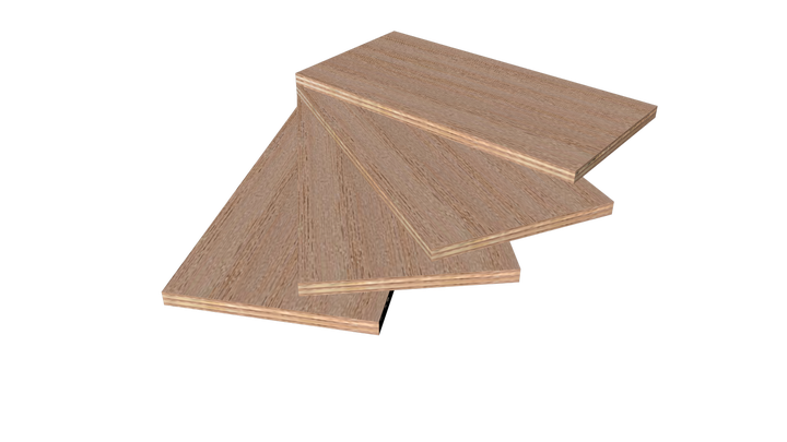
1. PCB composition
PCB contains two important components: Core and PP (Prepreg, semi-solid sheet).
Both surfaces of Core are covered with copper foil, which is used as a conductive layer, and the solid material is filled between the two surface layers, which is composed of reinforced material glass fiber impregnated with solid resin.
There is no copper foil on the surface of PP. It is composed of semi-solid resin and glass fiber, which is softer than Core. It constitutes the so-called wetting layer, which mainly acts as a filling in PCB to bond the core board Core. During factory production, the wetting layer generally cannot exceed 3 PP (the thickness is about 20mil). Due to the semi-solid characteristics of PP, the thickness of PP in each completed PCB will also deviate, so there may also be deviations in the consistency of impedance control.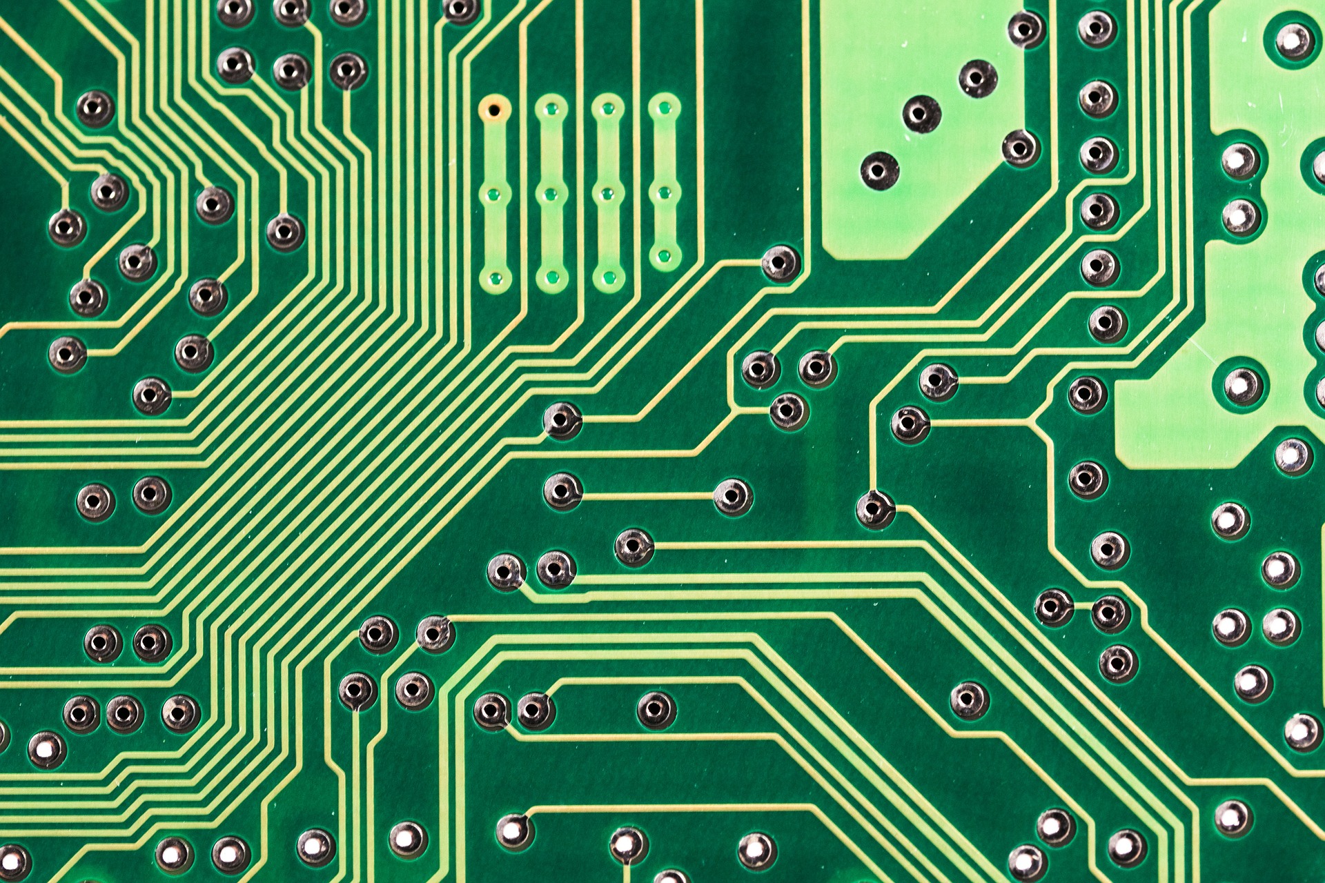
Use Core and PP together to realize the design and manufacture of multi-layer PCB.
2. Copper foil
The thickness of copper foil is often expressed in ounces (oz), which is a unit of mass (everyone understands gold and silver). 1oz of copper foil means that 1oz of copper foil (28.35g) is spread evenly on an area of 1 square foot , its thickness is 1.37mil, about 1.4mil=35um.
Copper foil materials commonly used in circuit boards are mainly divided into rolled copper foil and electrolytic copper foil. Rolled copper foil has tight molecules, smoother surface (favorable for high-speed signal transmission), good folding resistance and flexibility, and is not easy to break, so it is generally used For products with bending requirements.
3. PCB board
The most used PCB board is FR4, which uses glass fiber cloth as a reinforcing material and epoxy resin as an adhesive.
The other is the composite substrate CEM1, which is widely used in household appliances and other industries. It uses wood pulp fiber paper or cotton pulp fiber paper as the core reinforcement material, and glass fiber cloth as the surface layer reinforcement material. Both are impregnated with flame-retardant epoxy resin. resin. This board is mainly used in single-panel occasions. Its mechanical strength is lower than that of FR4 sheet, but the price is relatively cheaper, and it also has flame retardant properties.
The main parameters of PCB materials are relative permittivity and material loss angle. The combination of the two can represent the complex permittivity. It is mentioned in /126633951, from which it can be seen that the larger the relative permittivity, the slower the propagation speed of the signal in the medium; the larger the material loss angle, the greater the dielectric loss. Therefore, in high-speed signal PCB design, materials with small dielectric constant and material loss angle will be selected as much as possible, and the cost will increase accordingly.
4. PCB stack structure and impedance design
Common signal impedance types include single-ended 50 ohms, differential 100 ohms, single-ended radio frequency 50 ohms, etc. Impedance parameters can be calculated by software Si9000, which will not be described in detail in this article. A separate article on common impedance calculations will be written later to explain . One point that needs special mention is the 50 ohm impedance control of the single-ended RF line. The RF line generally runs on the surface (the purpose is to go out directly without punching holes to reduce the possibility of discontinuous impedance changes, and the surface signal speed is fast). Moreover, in order to enhance the anti-interference ability and reduce loss, the radio frequency line needs a thicker line width than ordinary signals, generally at least 15mil. In the previous article, we know that when the control characteristic impedance remains unchanged, the distance between the signal line and the reference layer must be increased while increasing the line width, so the RF line on the surface needs to refer to the third layer on the other layer, and the RF line on the surface layer The second layer below the line is hollowed out.
The most commonly used PCB stacks are 12 layers, 8 layers and 6 layers, and more than 20 layers have been encountered. In general, in a slightly larger company, PCB layout and schematic design are done by different people, but this does not mean that hardware engineers do not need to understand PCB-related knowledge, on the contrary, many times layout engineers It's not clear which signals are most important on the board and which are less important. Therefore, it is best for the hardware engineer to indicate the attention points of the signal in the layout on the schematic diagram, and actively communicate with the layout engineer to point out the problem points to assist them in the change. This requires hardware engineers to be more aware of the knowledge points related to PCB layout in order to provide effective guidance.
In actual work, the number of layers of multilayer boards is generally determined by the layout engineer, and the thickness is generally 1.6mm or 2mm. If there are no special requirements, the boards are mostly FR4. There are some basic principles for PCB stacking settings, which are of great benefit to improving the quality of signal integrity. We can check whether the design given by the Layout engineer is reasonable according to these principles, and put forward suggestions for improvement.
(1) The power plane and the ground plane are as close as possible, preferably adjacent, because two complete planes can form a large plane capacitor, which is equivalent to increasing the decoupling capacitor, reducing the impedance of the power supply to the ground, and is conducive to power integrity PI (PDN). In actual PCB design, it is difficult to make all power planes and ground planes adjacent, but generally the two adjacent stacked layers in the center can be set as power planes and ground planes, such as the 4th and 5th layers of an 8-layer board , The 6th and 7th layers of the 12-layer board are closely adjacent to each other and have a good coupling effect. If there are many types of power supply in a certain power layer in the design, the power layer will be divided into fragments. You can set the power layer close to the ground layer to obtain a relatively good capacitive coupling effect. For example, layer 6 is GND, layer 7 The layer is set as a piecemeal power layer with many types of power sources. Common and better stacking distribution structures for 8-layer boards and 12-layer boards are shown in Figure 1 and Figure 2 respectively (stack management in Altium Designer, if you use allegro, you can intuitively give impedance according to the stack settings), the thickness of the stack in the figure Not yet optimized for impedance control.
Figure 1 Commonly used stacking assignments for 8-layer boards
Figure 2 Commonly used stacking assignments for 12-layer boards
(2) All signal layers (especially key signals) should be adjacent to complete planes (both power and ground planes) as much as possible to ensure a complete and reliable return plane and impedance continuity. Special care should be taken to avoid cross-segmentation for high-speed signals. When the signal returns, it will automatically select the path with the least impedance of the driving path as the return path (forming a transmission line structure).
(3) When changing the signal layer, it is best not to change the reference layer; Secondly, if the reference layer is changed, it is best not to change the network properties of the reference layer. When changing the signal layer, add and reference layer near the signal via. If the signal layer changes, the network properties of the reference layer will also change. Vias with the same net properties have been mentioned in the previous MIPI article on PCB vias; it is best to keep the two reference layers as close as possible. These measures are all to ensure that the impedance of the return path remains as continuous as possible, and the interlayer impedance is as low as possible, thereby reducing signal voltage drop and signal distortion.
(4) Try to avoid two signal layers (including two power layers) adjacent to each other to reduce crosstalk. If it is really unavoidable, adjacent signal layers should be routed orthogonally, with one layer horizontally routed and one layer vertically routed.