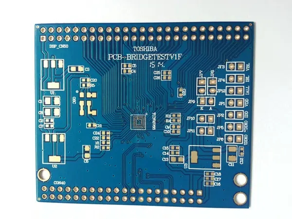
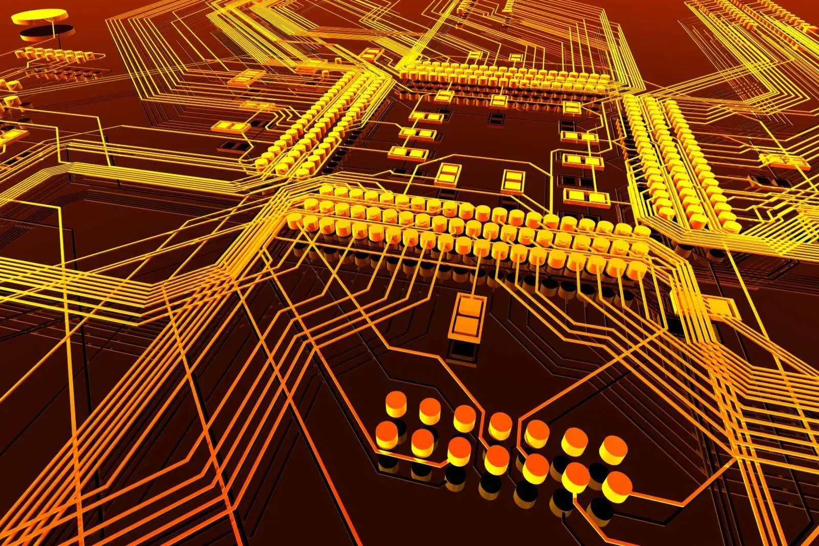
How to optimize the electromagnetic compatibility of PCB design
PCB manufacturers, PCB designers and PCBA manufacturers explain how to optimize the electromagnetic compatibility of PCB design


PCB manufacturers, PCB designers and PCBA manufacturers explain how to optimize the electromagnetic compatibility of PCB design
Circuit board manufacturing, circuit board design, PCBA processing manufacturer's right-hand assistant software to explain circuit board PCB design
Circuit board manufacturers, circuit board designers and PCBA manufacturers explain to you the major mistakes that need to be aware of in circuit board design
Circuit board manufacturing, circuit board design and PCBA processing manufacturers explain schematic simulation: a way to reduce PCB design errors and improve efficiency
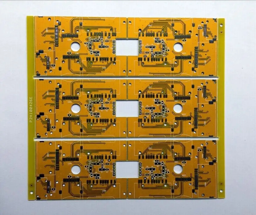
PCB manufacturers, PCB designers and PCBA manufacturers will explain the PCB design of intelligent wearable devices: smart bracelets
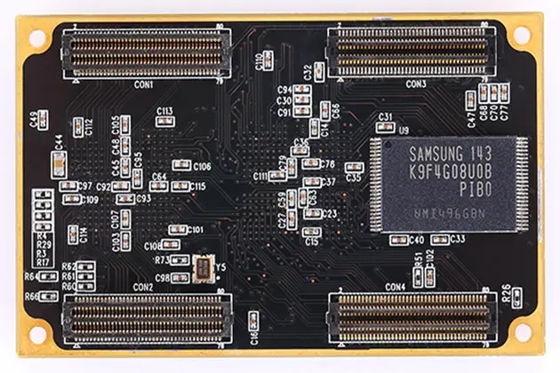
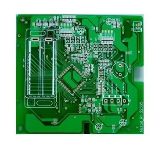
Understand PCB design, PCB layout and PCB manufacturing in PCB related industries and Let's see how pcb reverse development design works
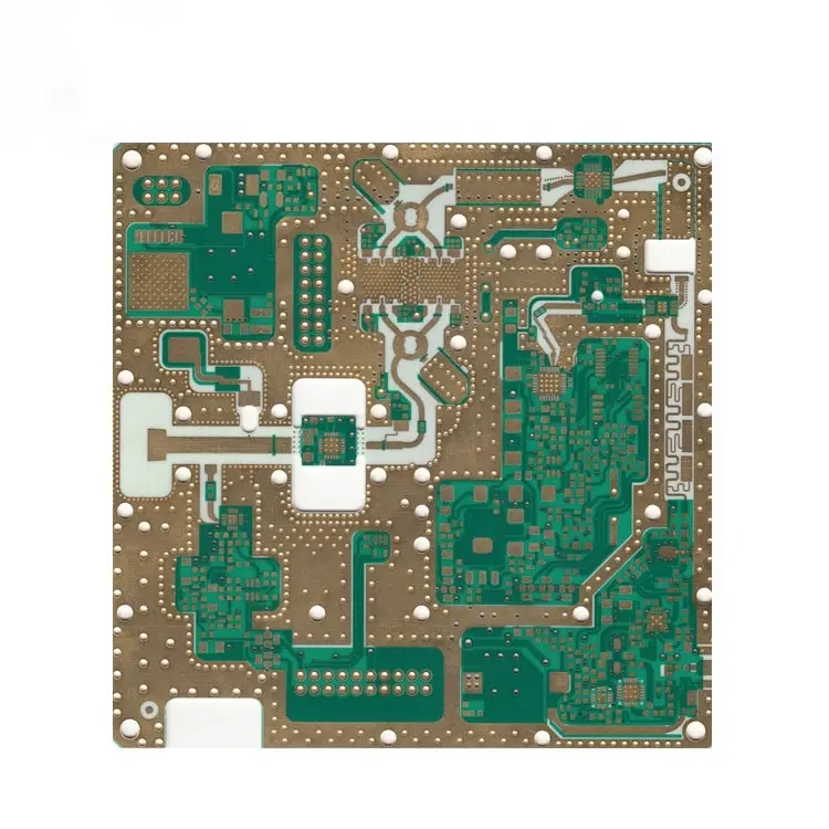
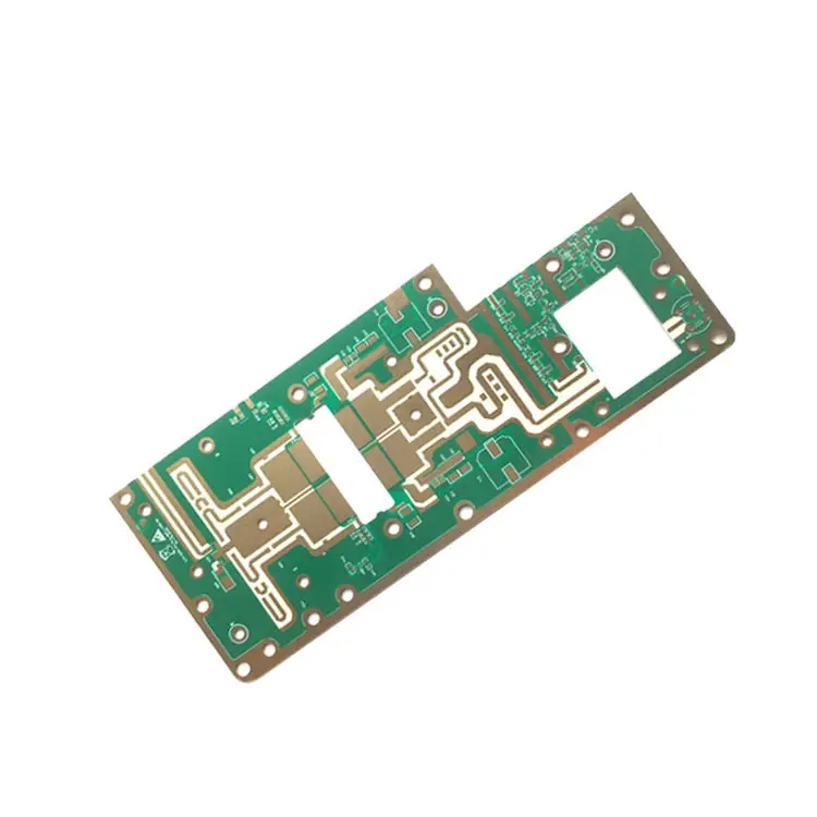
Understand PCB design, PCB layout and PCB manufacturing in PCB related industries and Explain the rf pcb design of pcb engineers in detail
Understand PCB design, PCB layout and PCB manufacturing in PCB related industries and Outline the design criteria of pad in pcb design
Circuit board manufacturing, circuit board design, PCBA manufacturers will explain the mechanical design of PCB wiring and the installation requirements of circuit boards
PCB manufacturers, PCB designers and PCBA manufacturers explain the detailed inspection work after PCB wiring
PCB manufacturer, PCB designer and PCBA manufacturer explain three special PCB wiring sharing and inspection methods
PCB manufacturers, PCB designers and PCBA manufacturers explain how to improve your design speed: IC replacement skills in PCB circuit design


