
Professional PCB manufacturing and assembly
Building 6, Zone 3, Yuekang Road,Bao'an District, Shenzhen, China
+86-13410863085Mon.-Sat.08:00-20:00

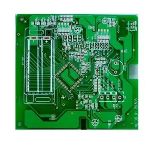
Detailed description of project inspection after PCB wiring
PCB manufacturers, PCB designers and PCBA manufacturers explain the detailed inspection work after PCB wiring
Is the pcb finished after wiring? Apparently not! The post PCB wiring inspection is also necessary, so how to check the wiring in PCB design to pave the way for later design? See below!
General PCB design drawing inspection items
1) Have you analyzed the circuit? Is the signal circuit divided into basic units for smoothing?
2) Is it allowed to use short or isolated key leads in the circuit?
3) Are the areas that must be shielded effectively?
4) Has the basic grid graphics been fully utilized?
5) Is the size of the printed circuit board the optimal size?
6) Do you want to use the selected wire width and spacing as much as possible?
7) Are the preferred pad sizes and hole sizes used?
8) Are photographic plates and sketches suitable?
9) Are the minimum jumpers used? Do jumpers go through components and accessories?
L0) Is the letter visible after assembly? Is the size and model correct?
11) Have large areas of copper foil been opened to prevent blistering?
12) Is there a tool locating hole?
PCB electrical characteristics inspection items:
1) Whether the influence of conductor resistance, inductance and capacitance is analyzed? Especially for the critical voltage drop phase grounding?
2) Whether the spacing and shape of wire accessories meet the insulation requirements?
3) Are insulation resistance values controlled and specified at key points?
4) Are polarities adequately identified?
5) Has the influence of wire spacing on leakage resistance and voltage been measured from the perspective of geometry?
6) Has the medium for changing the surface coating been identified?
PCB physical characteristics inspection items:
1) Are all pads and their locations suitable for final assembly?
2) Can the assembled PCB meet the shock and vibration work conditions?
3) What is the spacing between the specified standard elements?
4) Are loosely mounted components or heavier components secured?
5) Is the heat dissipation and cooling of heating elements correct? Or is it isolated from the printed circuit board and other thermal components?
6) Are voltage dividers and other multi lead components positioned correctly?
7) Are elements arranged and oriented for easy inspection?
8) Are all possible interferences on the printed circuit board and the entire printed circuit board assembly eliminated?
9) Is the size of the locating hole correct?
10) Are the tolerances complete and reasonable?
11) Have the physical properties of all coatings been controlled and signed?
12) Is the hole to lead diameter ratio within the acceptable range?
PCB manufacturers, PCB designers and PCBA manufacturers explain the detailed inspection work after PCB wiring


Just upload Gerber files, BOM files and design files, and the KINGFORD team will provide a complete quotation within 24h.