
Professional PCB manufacturing and assembly
Building 6, Zone 3, Yuekang Road,Bao'an District, Shenzhen, China
+86-13410863085Mon.-Sat.08:00-20:00


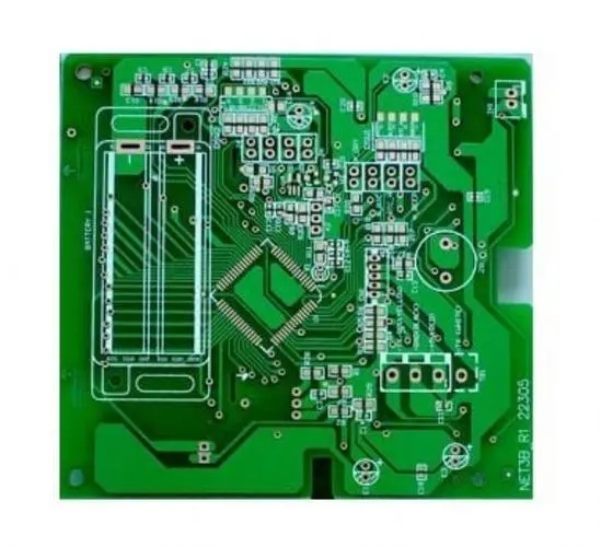
Mechanical design of PCB wiring and explanation of PCB installation requirements
PCB mechanical design factors:
Although printed circuit board adopts mechanical method to support components, it cannot be used as a structural member of the whole equipment. A certain amount of text support shall be provided at least every 5 inches at the edge of the printed board. The following factors must be considered when selecting and designing printed circuit boards:;
1) Structure of printed circuit board -- size and shape.
2) Type of mechanical accessories and plugs (sockets) required.
3) Adaptability of the circuit to other circuits and environmental conditions.
4) Consider installing the printed circuit board vertically or horizontally according to some factors, such as heating and dust.
5) Some environmental factors that need special attention, such as heat dissipation, ventilation, impact, vibration and humidity. Dust, salt spray and radiation.
6) The degree of support.
7) Hold and secure.
8) Easy to remove.
Installation requirements for PCB printed circuit board:
It shall be supported at least within 1 inch of the three edge edges of the printed circuit board. According to practical experience, the spacing of support points of printed circuit board with thickness of 0.031 -- 0.062 inch shall be at least 4 inches; For printed circuit boards with a thickness greater than 0.093 inch, the spacing between their supporting points shall be at least 5 inches. This measure can improve the rigidity of the printed circuit board and destroy the possible resonance of the printed circuit board.
The installation technology of certain printed circuit boards can be determined after considering the following factors.
1) Dimensions and shapes of printed circuit boards.
2) Number of input and output terminals.
3) Available equipment space.
4) Desired handling convenience.
5) The type of attachment to be installed.
6) Required heat dissipation.
7) Shieldability required.
8) The type of circuit and its relationship with other circuits.
Pulling out requirements of printed circuit board:
1) The area of the printed circuit board that does not require components to be installed.
2) The influence of plugging tools on the installation distance between two printed circuit boards.
3) The mounting holes and slots shall be specially prepared in the design of printed circuit boards.
4) When inserting and pulling tools are to be used in the equipment, especially its size shall be considered.
5) A plug and pull device is required, which is usually permanently fixed to the printed circuit board assembly with rivets.
6) In the mounting frame of printed circuit board, special design such as load bearing flange is required.
7) Adaptability of the used plug and pull tools to the size, shape and thickness of the printed circuit board.
8) The cost involved in using the plug and pull tool includes both the price of the tool and the increased expenditure.
9) In order to fasten and use the plug and pull tools, it is required to enter the equipment to a certain extent.
PCB mechanical considerations:
The characteristics of the substrate that have an important impact on the printed circuit assembly are: water absorption, thermal expansion coefficient, heat resistance, flexural strength, impact strength, tensile strength, shear strength and hardness.
All these characteristics not only affect the function of PCB structure, but also affect the productivity of PCB structure.
For most applications, the dielectric substrate of printed circuit board is one of the following substrates:
1) Phenolic impregnated paper.
2) Acrylic polyester impregnated glass felt with irregular arrangement.
3) Epoxy impregnated paper.
4) Epoxy impregnated glass cloth.
Each substrate can be flame retardant or combustible. The above 1, 2 and 3 can be punched. The most commonly used material of metallized hole printed circuit board is epoxy glass cloth. Its dimensional stability is suitable for high-density circuits, and it can minimize the occurrence of cracks in metallized holes.
One disadvantage of epoxy glass cloth laminate is that it is difficult to punch within the common thickness range of printed circuit board. For this reason, all holes are usually drilled out, and profiling milling is used to form the shape of printed circuit board.
PCB electrical considerations:
In DC or low-frequency AC occasions, the most important electrical characteristics of insulation substrate are insulation resistance, electrical isolation, printed wire resistance and breakdown strength.
In high-frequency and microwave applications, it is dielectric constant, capacitance and dissipation factors.
In all applications, the current load capacity of printed wire is important.
Wire drawing:
PCB wiring path and positioning
The printed wire shall follow the shortest route between components under the restriction of specified wiring rules. The coupling between parallel conductors shall be limited as far as possible. Good design requires the minimum number of layers for wiring, and the widest wire and the largest pad size are also required to be used under the corresponding packaging density. Because rounded corners and smooth inner corners may avoid some electrical and mechanical problems, sharp corners and sharp corners in wires should be avoided.
PCB width and thickness:
Current carrying capacity of copper conductor etched on rigid printed circuit board. For 1 oz and 2 oz conductors, 10% of the nominal value (in load ammeter) is allowed to be reduced, taking into account the etching method, normal changes in copper foil thickness and temperature difference; For printed circuit board assemblies coated with protective layer (substrate thickness less than 0.032 inch, copper foil thickness more than 3 ounces), the components are reduced by 15%; For the soldered printed circuit board, 30% reduction is allowed.
PCB wire spacing:
The minimum spacing of conductors must be determined to eliminate voltage breakdown or flashover between adjacent conductors. The spacing is variable and depends on the following factors:
1) Peak voltage between adjacent conductors.
2) Atmospheric pressure (maximum working height).
3) Coating used.
4) Capacitive coupling parameters.
The key impedance components or high-frequency components are generally placed very close to reduce the key stage delay. The transformer and inductive element shall be isolated to prevent coupling; Inductive signal conductors shall be arranged at right angles; Components that will generate any electrical noise due to magnetic field movement shall be isolated or rigidly mounted to prevent excessive vibration.
PCB wire pattern check:
1) Is the wire short and straight without sacrificing function?
2) Are the wire width limits observed?
3) Is the minimum conductor spacing that must be guaranteed reserved between conductors, between conductors and mounting holes, between conductors and bonding pads?
4) Are parallel runs of all wires (including component leads) closer together avoided?
5) Is acute angle (90 ℃ or less) avoided in wire drawing?
PCB design item check list:
1) Check the rationality and correctness of the schematic diagram;
2) Check the correctness of component packaging of schematic diagram;
3) Spacing between strong and weak current, spacing between isolated areas;
4) Check the corresponding schematic diagram and PCB diagram to prevent the loss of network table;
5) Whether the package of components is consistent with the real object;
6) Whether the placement of components is appropriate:
7) Whether the elements are easy to install and disassemble;
8) Whether the temperature sensing element is too close to the heating element;
9) Whether the distance and direction of mutual inductance components are appropriate;
10) Whether the connectors are placed smoothly;
11) Easy to plug and unplug;
12) Input and output;
13) Strong current and weak current;
14) Whether digital and analog are interlaced;
15) Arrangement of upwind and downwind components;
16) Whether the directional components are wrongly turned instead of rotated;
17) Whether the installation holes of element pins are suitable and easy to insert;
18) Check whether the empty pin of each component is normal and whether it is a leaky line;
19) Check whether there are vias in the upper and lower layers of the same network table, and the bonding pads are connected through the holes to prevent wire breakage and ensure the integrity of the lines;
20) Check whether the upper and lower characters are placed correctly and reasonably. Do not put components to cover the characters, so as to facilitate the operation of welding or maintenance personnel;
21) The connection of the very important upper and lower layers of wires should not only be connected by the pad of the directly inserted component, but also by the via;
22) The arrangement of power supply and signal line in the socket shall ensure the integrity and anti-interference of the signal;
23) Pay attention to the proper proportion of pads and holes;
24) All plugs shall be placed on the edge of PCB board as far as possible and easy to operate;
25) Check whether the component label is consistent with the component, and all components shall be placed in the same direction and orderly as far as possible;
26) The power supply and ground wire shall be thickened as much as possible without violating the design rules;
27) Generally, the upper layer shall be laid with horizontal lines and the lower layer shall be laid with vertical lines, and the chamfer shall not be less than 90 degrees;
28) Whether the size and distribution of the mounting holes on the PCB are appropriate, and minimize the bending stress of the PCB;
29) Pay attention to the high and low distribution of components on PCB and the shape and size of PCB to ensure convenient assembly.
PCB manufacturers, PCB designers and PCBA manufacturers will explain the mechanical design of PCB wiring and the installation requirements of PCB.
Outline the design criteria of pad in pcb design
Nov 12,2022


Just upload Gerber files, BOM files and design files, and the KINGFORD team will provide a complete quotation within 24h.