
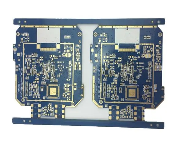
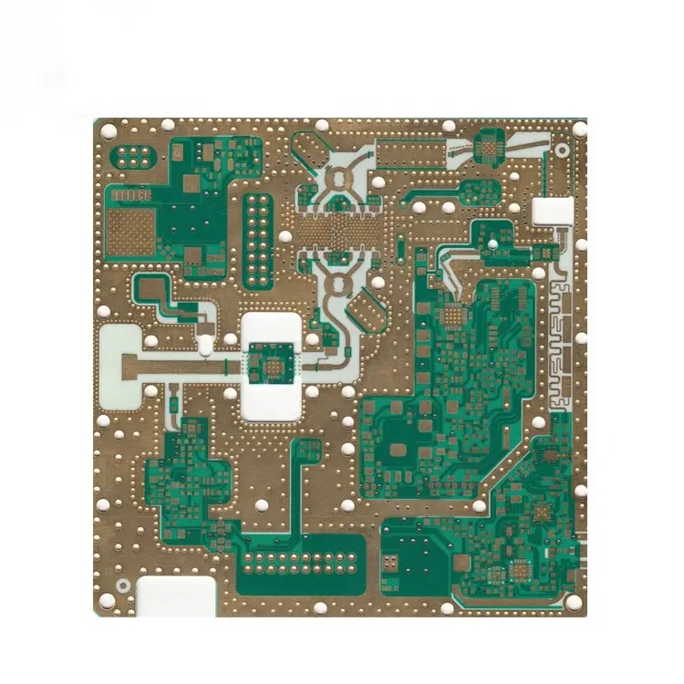
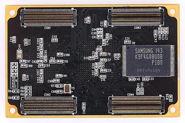
Professional PCB manufacturing and assembly
Building 6, Zone 3, Yuekang Road,Bao'an District, Shenzhen, China
+86-13410863085Mon.-Sat.08:00-20:00

Software explanation of right-hand man for PCB design
What is Protel
Protel is a drawing software in the electronic industry, which is used to draw circuit boards and schematic diagrams. For example, the TV we use has a circuit board, which is made by Protel software or other similar software; The TV is often equipped with a schematic diagram (convenient for maintenance), which is also drawn by this software.
PCB drawing software was originally produced by Protel, but it disappeared after upgrading to Protel99se. Later, the company changed its name, and the new software was DXP2004. Later, AD9 and AD10 were produced. Now most large companies use AD9 or AD10.
At the end of 2005, the original manufacturer of PROTEL Tutorial Protel software, AlTIum Company, launched the latest high-end version of Protel series, AlTIum Designer 6.0. AlTIum Designer 6.0, a new version of the fully integrated electronic product development system, is the first and only complete board level design solution in the industry. AlTIum Designer is the first product in the industry to integrate the design process, integrated PCB design, programmable device (such as FPGA) design and embedded software development function based on processor design. It is a solution for simultaneous PCB and FPGA design and embedded design. It has all the functions required to transform the design scheme from concept to final product.
Altium Designer 6, the latest high-end version, not only fully inherits the functions and advantages of previous versions including 99SE and Protel2004, but also adds many improvements and high-end functions. Altium Designer 6.0 broadens the traditional boundaries of board level design, fully integrates FPGA design functions and SOPC design implementation functions, thus allowing engineers to integrate FPGA, PCB design and embedded design in system design.
Protel Key Features
Protel99 is a pure 32-bit circuit design plate making system based on Win95/Win NT/Win98/Win2000. Protel99 provides an integrated design environment, including schematic design and PCB wiring tools, integrated design document management, and support for workgroup collaborative design through the network.
The main features of Protel99 are as follows:
(1) Protel99 system has made pure 32-bit code optimization for Windows NT4/9X, making Protel99 design system stable and efficient.
(2) SmartTool technology integrates all design tools in a single design environment.
(3) SmartDoc (intelligent document) technology stores all design data files in a single design database and uses the design manager to manage them uniformly. Design the database to Ddb is a suffix and is managed uniformly in the Design Manager. The documents uniformly managed by the Design Manager are newly proposed in Protel99, not in previous versions.
(4) SmartTeam technology enables multiple designers to design the same design separately through network security, and then integrate each part into the design manager through the workgroup management function.
(5) The compound option of PCB automatic routing rule conditions greatly facilitates the design of routing rules.
(6) Support integrated rule driven PCB routing with online rule checking function.
(7) The inherited PCB automatic routing system uses the latest artificial intelligence technologies, such as artificial neural network, fuzzy expert system, fuzzy theory and fuzzy neural network. Even for very complex circuit boards, the routing results can reach the expert level.
(8) Two different layout methods are adopted for automatic layout of PCB design, namely Cluster Placer and Statistical Placer. In previous versions, only statistics based layouts were provided.
(9) Protel99 has added the design function of automatic layout rules. The Placement tab is newly added in Protel99 to set automatic layout rules.
(10) Enhanced interactive layout and routing modes, including "Push and choose".
(11) The circuit board signal integrity rule design and inspection function can detect potential impedance matching, signal propagation delay, signal overload and other problems. The Signal Integrity tab is also newly added in Protel99 to design rules related to signal integrity.
(12) The introduction of part encapsulation class generator improves the management function of part encapsulation.
(13) Extensive integrated wizard functions guide designers to complete complex work.
(14) The update function from schematic diagram to printed circuit board strengthens the connection between Sch and PCB.
(15) It fully supports plate making output and generation of NC processing code files for circuit boards.
(16) A wide range of device libraries can be upgraded through Protel Library Development Center.
(17) You can use standard or user-defined templates to generate new schematic files.
(18) The integrated schematic design system has collected more than 60000 components.
(19) Through the complete SPICE 3f5 simulation system, the signal can be directly simulated in the schematic diagram.
(20) You can select more than 60 industrial standard computer circuit board wiring templates or you can generate a circuit board template yourself.
(21) Protel99's open document function enables users to conduct three times of development through API calls.
(22) The integrated macro programming function supports the use of Client Basic programming language.
Common shortcut keys of Protel
PageUp: Zoom in with the mouse as the center
PageDown: Zoom out with the mouse as the center.
Home: Center the mouse position
End: Refresh (redraw)
*: Switch between the top layer and the bottom layer
+(-) Switch layer by layer: "+" is opposite to "-"
Unit switching between Qmm and mil
IM: Measure the distance between two points
Ex: edit X, X is the edit target, and the code is as follows: (A)=arc; (C) =element; (F) =filled; (P) =pad; (N) =network; (S) =character; (T) =conductor; (5) =via; (1) =connecting line; (G) =Fill polygons. For example, when pressing EC to edit a component, the mouse pointer will display a "cross", and click the component to edit.
Px: Place X as the placement target, and the code is the same as above.
Mx: move X, X is the moving target, (A), (C), (F), (P), (S), (T), (V), (G) are the same as above, and (I)=flip the selected part; (O) Rotate the selected part; (M) =Move the selected part; (R) =Re route.
Sx: select X, where X is the selected content, and the code is as follows: (I)=internal area; (O) =external area; (A) =All; (50) =all on the layer; (K) =locking part; (N) =physical network; (C) =physical connection line; (H) =pad with specified aperture; (G) =Pads outside the grid. For example, if you want to select All, press SA, and all figures are highlighted to indicate that they have been selected, you can copy, clear, and move the selected files.
The PCB manufacturer, PCB designer and PCBA manufacturer will explain the powerful assistant software for PCB design.


Just upload Gerber files, BOM files and design files, and the KINGFORD team will provide a complete quotation within 24h.